Smctac65n16, Solidtron – Silicon Power SMCT AC 65N14_N-MOS VCS, Bare Die User Manual
Page 5
Solidtron
TM
N-MOS VCS, Bare Die
Data Sheet (Rev 0 - 10/28/10)
SMCTAC65N16
275 Great Valley Parkway
Malvern, PA 19355
Ph: 610-407-4700
A1.
Use of Gate Return Bond Area.
The MCT is designed for high di/dt applications. An independent cathode connection or "Gate Return Bond Area" was provided to
minimize the effects of rapidly changing Anode-Cathode current on the Gate control voltage, (V=L*di/dt). It is therefore, critcal that the
user utilize the Gate Return Bond Area as the point at which the gate driver reference (return) is attached to the VCS device.
Solidtron
TM
N-MOS VCS, Bare Die
Data Sheet (Rev 0 - 10/28/10)
SMCTAC65N16
275 Great Valley Parkway
Malvern, PA 19355
Ph: 610-407-4700
Note: All product specifications and data are subject to change without notice. The device specifications
listed in this datasheet may not be considered as an assurance of the component characteristics.
Devices will need to be tested and qualified in their respective applications. Depending on the
application adjustments to the data contained in this datasheet may be necessary. The use of Silicon
Power products in medical, life‐saving, or life‐sustaining applications and systems is subject to prior
specification and written approval by Silicon Power. We therefore strongly recommend prior
Packaging and Handling
A1.
Use of Gate Return Bond Area.
The MCT is designed for high di/dt applications. An independent cathode connection or "Gate Return Bond Area" was provided to
minimize the effects of rapidly changing Anode-Cathode current on the Gate control voltage, (V=L*di/dt). It is therefore, critcal that the
user utilize the Gate Return Bond Area as the point at which the gate driver reference (return) is attached to the VCS device.
Solidtron
TM
N-MOS VCS, Bare Die
Data Sheet (Rev 0 - 10/28/10)
SMCTAC65N16
275 Great Valley Parkway
Malvern, PA 19355
Ph: 610-407-4700
Note: All product specifications and data are subject to change without notice. The device specifications
listed in this datasheet may not be considered as an assurance of the component characteristics.
Devices will need to be tested and qualified in their respective applications. Depending on the
application adjustments to the data contained in this datasheet may be necessary. The use of Silicon
Power products in medical, life‐saving, or life‐sustaining applications and systems is subject to prior
specification and written approval by Silicon Power. We therefore strongly recommend prior
consultation of our personal.
Packaging and Handling
A1.
Use of Gate Return Bond Area.
The MCT is designed for high di/dt applications. An independent cathode connection or "Gate Return Bond Area" was provided to
minimize the effects of rapidly changing Anode-Cathode current on the Gate control voltage, (V=L*di/dt). It is therefore, critcal that the
user utilize the Gate Return Bond Area as the point at which the gate driver reference (return) is attached to the VCS device.
1. The cathode and gate contact pads are metallized
with aluminum for aluminum wire bondable surfaces.
The anode bond area is metalized with a solderable
metal surfaces(plating meets IPC-4552 Specification for
Electroless Nickel/Immersion Gold (ENIG), 3 to 6 μm
[118.1 to 236.2 μin] Ni/ 0.05 μm minimum [1.97 μin
minimum] Au providing the user with a solderable
device.
Solidtron
TM
N-MOS VCS, Bare Die
Data Sheet (Rev 0 - 10/28/10)
SMCTAC65N16
275 Great Valley Parkway
Malvern, PA 19355
Ph: 610-407-4700
Note: All product specifications and data are subject to change without notice. The device specifications
listed in this datasheet may not be considered as an assurance of the component characteristics.
Devices will need to be tested and qualified in their respective applications. Depending on the
application adjustments to the data contained in this datasheet may be necessary. The use of Silicon
Power products in medical, life‐saving, or life‐sustaining applications and systems is subject to prior
specification and written approval by Silicon Power. We therefore strongly recommend prior
consultation of our personal.
A1.
Use of Gate Return Bond Area.
The MCT is designed for high di/dt applications. An independent cathode connection or "Gate Return Bond Area" was provided to
minimize the effects of rapidly changing Anode-Cathode current on the Gate control voltage, (V=L*di/dt). It is therefore, critcal that the
user utilize the Gate Return Bond Area as the point at which the gate driver reference (return) is attached to the VCS device.
1. The cathode and gate contact pads are metallized
with aluminum for aluminum wire bondable surfaces.
The anode bond area is metalized with a solderable
metal surfaces(plating meets IPC-4552 Specification for
Electroless Nickel/Immersion Gold (ENIG), 3 to 6 μm
[118.1 to 236.2 μin] Ni/ 0.05 μm minimum [1.97 μin
minimum] Au providing the user with a solderable
device.
2. This device must be coated or potted using a
dielectric material prior to subjecting to voltage above
1kV.
3. Installation reflow temperature should not exceed
350
o
C or device degradation may result.
4. Proper handling procedures must be observed to
prevent electrostatic discharge which may result in
t d
t th
t
f th d i
Solidtron
TM
N-MOS VCS, Bare Die
Data Sheet (Rev 0 - 10/28/10)
SMCTAC65N16
275 Great Valley Parkway
Malvern, PA 19355
Ph: 610-407-4700
Note: All product specifications and data are subject to change without notice. The device specifications
listed in this datasheet may not be considered as an assurance of the component characteristics.
Devices will need to be tested and qualified in their respective applications. Depending on the
application adjustments to the data contained in this datasheet may be necessary. The use of Silicon
Power products in medical, life‐saving, or life‐sustaining applications and systems is subject to prior
specification and written approval by Silicon Power. We therefore strongly recommend prior
consultation of our personal.
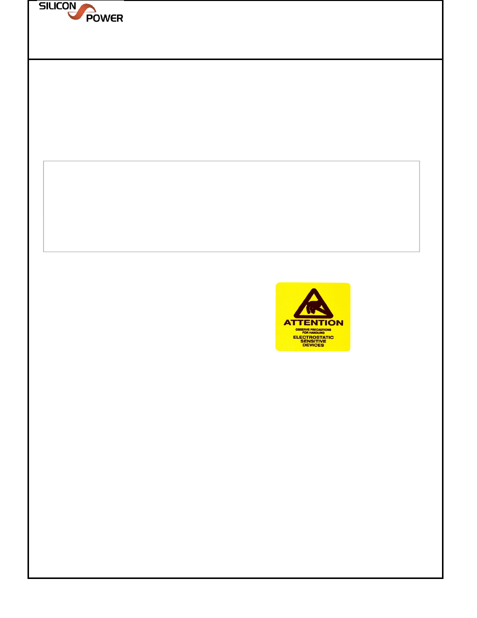
ATTENTION
OBSERVE PRECAUTIONS FOR HANDLING
ELECTROSTATIC DISCHARGE SENSITIVE
DEVICES IN ALL ASSEMBLY AND TEST AREAS
A1.
Use of Gate Return Bond Area.
The MCT is designed for high di/dt applications. An independent cathode connection or "Gate Return Bond Area" was provided to
minimize the effects of rapidly changing Anode-Cathode current on the Gate control voltage, (V=L*di/dt). It is therefore, critcal that the
user utilize the Gate Return Bond Area as the point at which the gate driver reference (return) is attached to the VCS device.
1. The cathode and gate contact pads are metallized
with aluminum for aluminum wire bondable surfaces.
The anode bond area is metalized with a solderable
metal surfaces(plating meets IPC-4552 Specification for
Electroless Nickel/Immersion Gold (ENIG), 3 to 6 μm
[118.1 to 236.2 μin] Ni/ 0.05 μm minimum [1.97 μin
minimum] Au providing the user with a solderable
device.
2. This device must be coated or potted using a
dielectric material prior to subjecting to voltage above
1kV.
3. Installation reflow temperature should not exceed
350
o
C or device degradation may result.
4. Proper handling procedures must be observed to
prevent electrostatic discharge which may result in
permanent damage to the gate of the device
Solidtron
TM
N-MOS VCS, Bare Die
Data Sheet (Rev 0 - 10/28/10)
SMCTAC65N16
275 Great Valley Parkway
Malvern, PA 19355
Ph: 610-407-4700
Note: All product specifications and data are subject to change without notice. The device specifications
listed in this datasheet may not be considered as an assurance of the component characteristics.
Devices will need to be tested and qualified in their respective applications. Depending on the
application adjustments to the data contained in this datasheet may be necessary. The use of Silicon
Power products in medical, life‐saving, or life‐sustaining applications and systems is subject to prior
specification and written approval by Silicon Power. We therefore strongly recommend prior
consultation of our personal.
ATTENTION
OBSERVE PRECAUTIONS FOR HANDLING
ELECTROSTATIC DISCHARGE SENSITIVE
DEVICES IN ALL ASSEMBLY AND TEST AREAS