Packaging and handling – Silicon Power CCS AC 43N40_N-Type Semiconductor Discharge Switch, Bare Die User Manual
Page 5
CCSAC43N40A10
N-Type Semiconductor Discharge Switch, Bare Die
5
Data Sheet (Rev 0- ##/##/####)
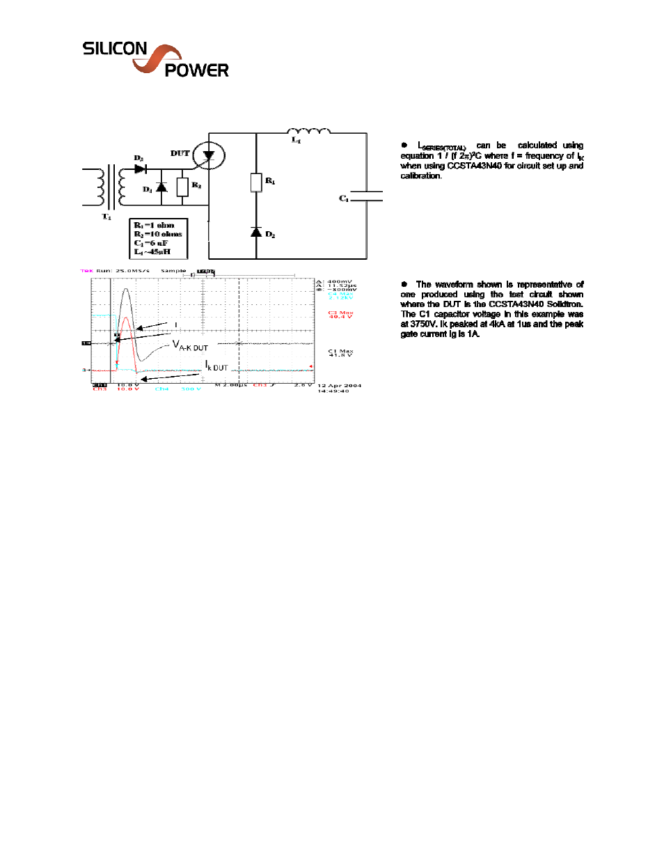
Figure 3: Typical test circuit and waveforms.
Packaging and Handling
1. ATTENTION OBSERVE PRECAUTIONS FOR HANDLING ELECTROSTATIC
DISCHARGE SENSITIVE DEVICES IN ALL ASSEMBLY AND TEST AREAS. Proper
handling procedures must be observed to prevent electrostatic discharge which may result in
permanent damage to the device.
2. The user is required to encapsulate the device in an encapsulant material prior to applying high
voltage. This prevents debris and contaminants from compromising the JTE area.
2. Use of a separate gate return path instead of the cathode power contact is recommended to
minimize the effects of rapidly changing Anode-Cathode currents.
3. Shorting resistor R
GK
is application specific. It can control the gate drive requirements and
some device properties. However, R
GK
= 10 Ohms satisfies most application requirements.
4. Installation reflow temperature should not exceed 320°C or device degradation may result.
Silicon Power Corporation
275 Great Valley Parkway
Malvern, PA 19355
Ph: 610-407-4700
Fax: 610-407-3688
www.siliconpower.com