Solidtron, N-mos vcs, thinpak, Performance characteristics – Silicon Power SMCT TA 65N14_N-MOS VCS, ThinPak User Manual
Page 2: Typical performance curves
Performance Characteristics
T
J
=25
o
C unless otherwise specified
Measurements
Parameters
Symbol
Test Conditions
Min.
Typ.
Max.
Units
Anode to Cathode Breakdown Voltage
V
(BR)
V
GK
=-5, I
A
=1mA
1400
V
Anode-Cathode Off-State Current
i
D
V
GE
=-5V, V
AK
=1200V
T
C
=25
o
C
<10
100
uA
T
C
=150
o
C
250
1000
uA
Gate-Cathode Turn-On Threshold Voltage
V
GK(TH)
V
AK
=V
GK
, I
AK
=1mA
0.7
V
Gate-Cathode Leakage Current
I
GK(lkg)
V
GK
=+/-20V
750
nA
Anode-Cathode On-State Voltage
V
T
I
T
=65A, V
GK
=+5V
T
C
=25
o
C
1.3
1.8
V
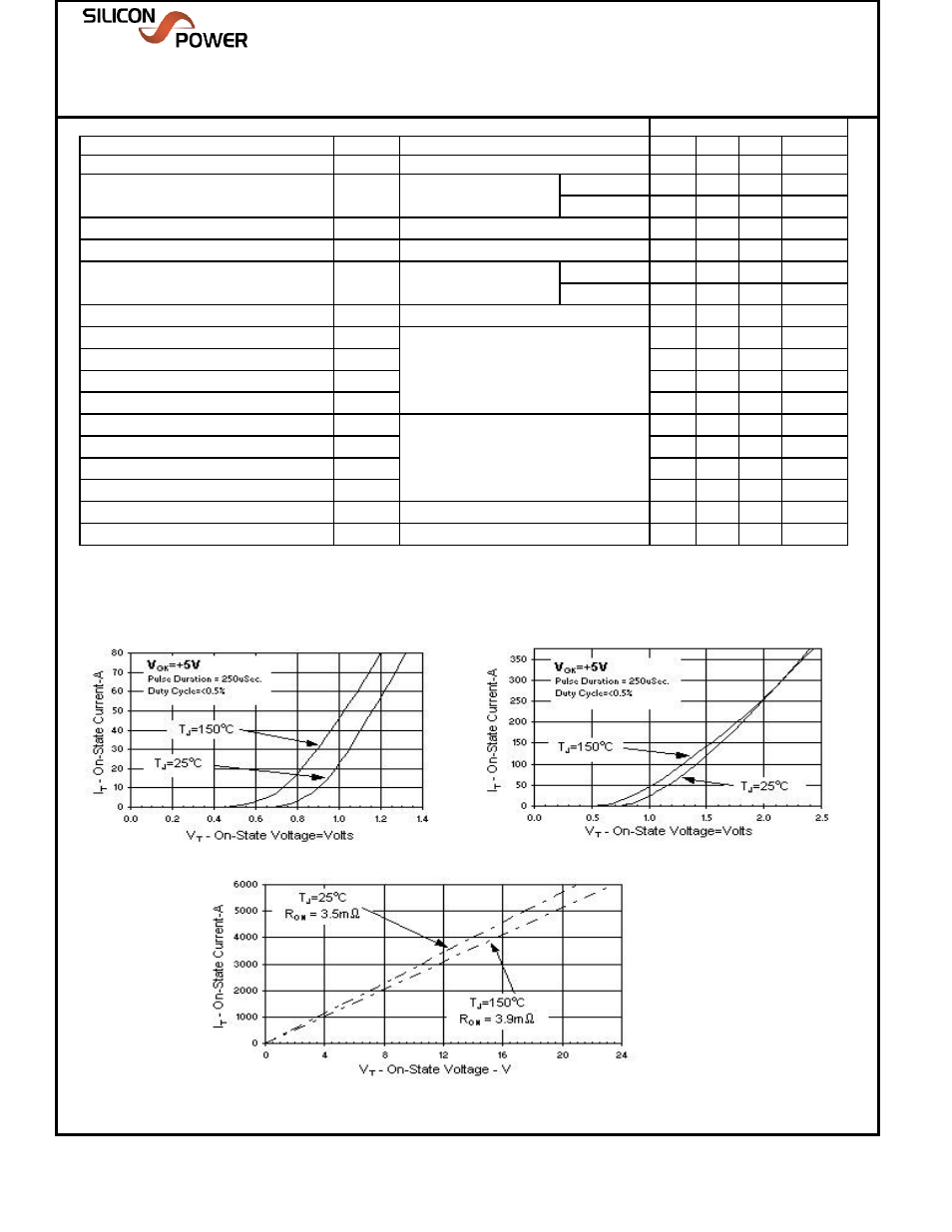
(See Figures 1,2 & 3)
T
C
=150
o
C
1.1
1.4
V
Input Capacitance
C
ISS
18
nF
Turn-on Delay Time
t
D(ON)
0.2uF Capacitor Discharge
82
150
nS
Rate of Change of Current
dI/dt
T
J
=25
o
C, V
GK
= -5V to +5V
58
kA/uSec
Peak Anode Current
I
P
V
AK
=800V, RG=4.7Ω
3300
A
Discharge Event Energy
E
DIS
L
S
= 8nH (See Figures 4,5 & 6)
36
mJ
Turn-on Delay Time
t
D(ON)
0.2uF Capacitor Discharge
64
120
nS
Rate of Change of Current
dI/dt
T
J
=150
o
C, V
GK
= -5V to +5V
100
kA/uSec
Peak Anode Current
I
P
V
AK
=1200V, RG=4.7Ω
5200
A
Discharge Event Energy
E
DIS
L
S
= 8nH (See Figures 4,5 & 6)
74
mJ
Junction to Case Thermal Resistance
R
θ
JC
Anode (bottom) side cooled (Note 1.)
0.035
o
C/W
Junction to Case Thermal Resistance
R
θ
JC
Cathode-Gate (top) side cooled (Note 2.)
0.6
o
C/W
Notes:
1. Case Exterior Assumed to be 0.002" of 63sn/37pb solder applied directly to Anode. (See Figure 7.)
Solidtron
TM
N-MOS VCS, ThinPak
Data Sheet (Rev 0 - 02/15/08)
SMCTTA65N14A10
275 Great Valley Parkway
Malvern, PA 19355
Ph: 610-407-4700
1. Case Exterior Assumed to be 0.002" of 63sn/37pb solder applied directly to Anode. (See Figure 7.)
2. Case Exterior Assummed to be 0.002" of 63sn/37pb solder applied directly to cathode bond area of thinPak. (See Figure 7.)
Typical Performance Curves
(unless otherwise specified)
Figure 1. On-State Characteristics
Figure 2. On-State Characteristics
Figure 3. Predicted High Current On-State Characteristics
CAO 05/28/09