Pcmcia i/o write access – AMD Am79C930 User Manual
Page 134
AMD
P R E L I M I N A R Y
134
Am79C930
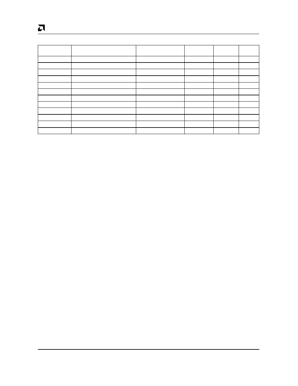
PCMCIA I/O WRITE ACCESS
Parameter
Symbol
Parameter Description
Test Conditions
Min
Max
Unit
t
AVIWL
Address setup to
IOWR
↓
70
ns
t
IWHAX
Address hold from
IOWR
↑
20
ns
t
RGLIWL
REG
setup to
IOWR
↓
5
ns
t
IWHRGH
REG
hold from
IOWR
↑
0
ns
t
ELIWL
CE
setup to
IOWR
↓
5
ns
t
IWHEH
CE
hold from
IOWR
↑
20
ns
t
IWLIWH
IOWR
width
165
ns
t
IWLWTL
WAIT
↓
delay from
IOWR
↓
35
ns
t
WTLWTH
WAIT
width
Notes 1, 2
53 X T
CLKIN
ns
t
WTHIWH
IOWR
↑
from
WAIT
↑
0
ns
t
DVIWL
Data setup to
IOWR
↓
60
ns
t
IWHDX
Data hold from
IOWR
↑
30
ns
Notes:
1. The max value for this parameter assumes the following worst case situation:
Value
Worst Case
0
FLASH and SRAM wait states set at “3.”
1
Host performs PCMCIA WRITE cycle at same time that Am79C930 embedded 80188 controller begins
instruction fetch cycle to FLASH memory.
2
PCMCIA WRITE cycle is posted internal to Am79C930 device, pending the completion of the embedded 80188
controller access.
3
Host performs PCMCIA READ cycle immediately following completion of PCMCIA WRITE cycle.
4
After completion of first embedded 80188 access to FLASH, posted PCMCIA WRITE executes to SRAM;
PCMCIISA READ stycle is being held in wait state.
5
After completion of posted PCMCIA WRITE cycle, new embedded 80188 access to FLASH begins.
6
After completion of second embedded 80188 access to FLASH, PCMCIA READ cycle is allowed to proceed onto
memory bus to SRAM; host is still held in wait state.
7
At SRAM READ cycle completion, data is delivered to PCMCIA bus and wait state is exited.
2. Parameter is not included in production test.