H40 absolute shock-proof encoder, Data transmission sequence, Interfacing long data lines – BEI Sensors H40 Absolute Shock Proof Encoder User Manual
Page 2: Serial synchronous interface (ssi), Bearing life vs. speed at various radial loads, Features, Ssi timing
Tel: 805-968-0782 /800-350-2727 | Fax: 805-968-3154 / 800-960-2726 | 7230 Hollister Ave., Goleta, CA 93117-2807
www.beisensors.com
H40 Absolute Shock-Proof Encoder
Notes
Options
Figure 1
1. Mounting is usually done either using the D-style
square flange mount, E- or G-style servo mounts, or
one of the standard face mounts, F1 for example.
Consult factory for additional face mount options.
2.The shaft seal is recommended in virtually all instal-
lations. The most common exceptions are applications
requiring a very low starting torque or those requiring
operation at both high temperature and high speed.
3. Non-standard index widths and multiple indices are
available by special order. Consult factory.
4. Complementary outputs are recommended for use
with line driver type (source/sink) outputs. When used
with differential receivers, this combination provides a
high degree of noise immunity.
5. Output IC’s: Output IC’s are available as either
Line Driver (LD) or NPN Open Collector (OC) types.
Open Collectors require pull-up resistors, resulting in
higher output source impedance (sink impedance is
similar to that of line drivers). In general, use of a
Line Driver style output is recommended. Line
Drivers source or sink current and their lower
impedance mean better noise immunity and faster
switching times.
Warning: Do not connect any line driver outputs
directly to circuit common/OV, which may damage
the driver. Unused outputs should be isolated and left
floating. Our applications specialists would be pleased
to discuss your system requirements and the compat-
ibility of your receiving electronics with Line Driver
type outputs.
28V/V:
Multi-voltage Line Driver (7272*): 100 mA source/
sink. Input voltage 5 to 28 VDC +/- 5% standard
(Note: V
out
= V
in
). This driver is TTL compatible when
used with 5 volt supply. Supply lines are protected
against overvoltage to 60 volts and reverse voltage.
Outputs are short circuit protected for one minute.
Supply current is 120 mA typical (plus load current).
This is the recommended replacement for 3904R and
7406R open collector outputs with internal pullup
resistors. It is also a direct replacement for any 4469,
88C30, 8830 or 26LS31 line driver
28V/5:
Multi-voltage Line Driver (7272*): 100 mA source/
sink. Input voltage 5 to 28 VDC +/- 5% standard,
internally regulated with 5V (TTL compatible) logic
out. Supply lines are protected against overvoltage to
60 volts and reverse voltage. Outputs are short circuit
protected for one minute. Supply current is 90 mA
typical (plus load current).
Note: Limit encoder load
to 2.5W max at ambient. Example at 12 VDC: 2.5W/
(+12VDC minus +5VDC) = 357 mA total allowed cur-
rent. Consult factory for your specific requirements.
28V/OC:
NPN Open Collector (3904*, 7273*). Current sink
of 80 mA max. Current sourced by external pull- up
resistor. Output can be pulled up to voltage other than
supply voltage (30 V max). Input voltage 5 to 28 VDC
+
/- 5% standard. Supply current is 120 mA typical.
This replaces prior IC’s with designations of 3904,
7406, 3302, 681 and 689.
6. Special –S at the end of the model number is used
to define a variety of non-standard features such as
special shaft lengths, voltage options, or special test-
ing. Please consult the factory to discuss your special
requirements.
7. Higher frequency response may be available.
Please consult with the factory.
8. Extended temperature ratings are available in the
following ranges:
-40 to 70°C, -40 to 85°C, –20 to 105°C and –40
to 105°C depending on the particular model. Some
models can operate down to -55°C. Extended tem-
perature ranges can affect other performance factors.
Consult with factory for more specific information.
9. Mating straight plug receptacles may be ordered
from
the factory:
For M12 use MS3116F12-10S,
For M14 use MS3106F14S-6S
For M14/19 use MS3116J14-19S,
For M16 use MS3106F16S-1S
For M18 use MS3106F18-1S,
For M20 use MS3106F20-29S
*
Products manufactured prior to April 2007 used the line driver IC number instead of volt-
age output in model number.
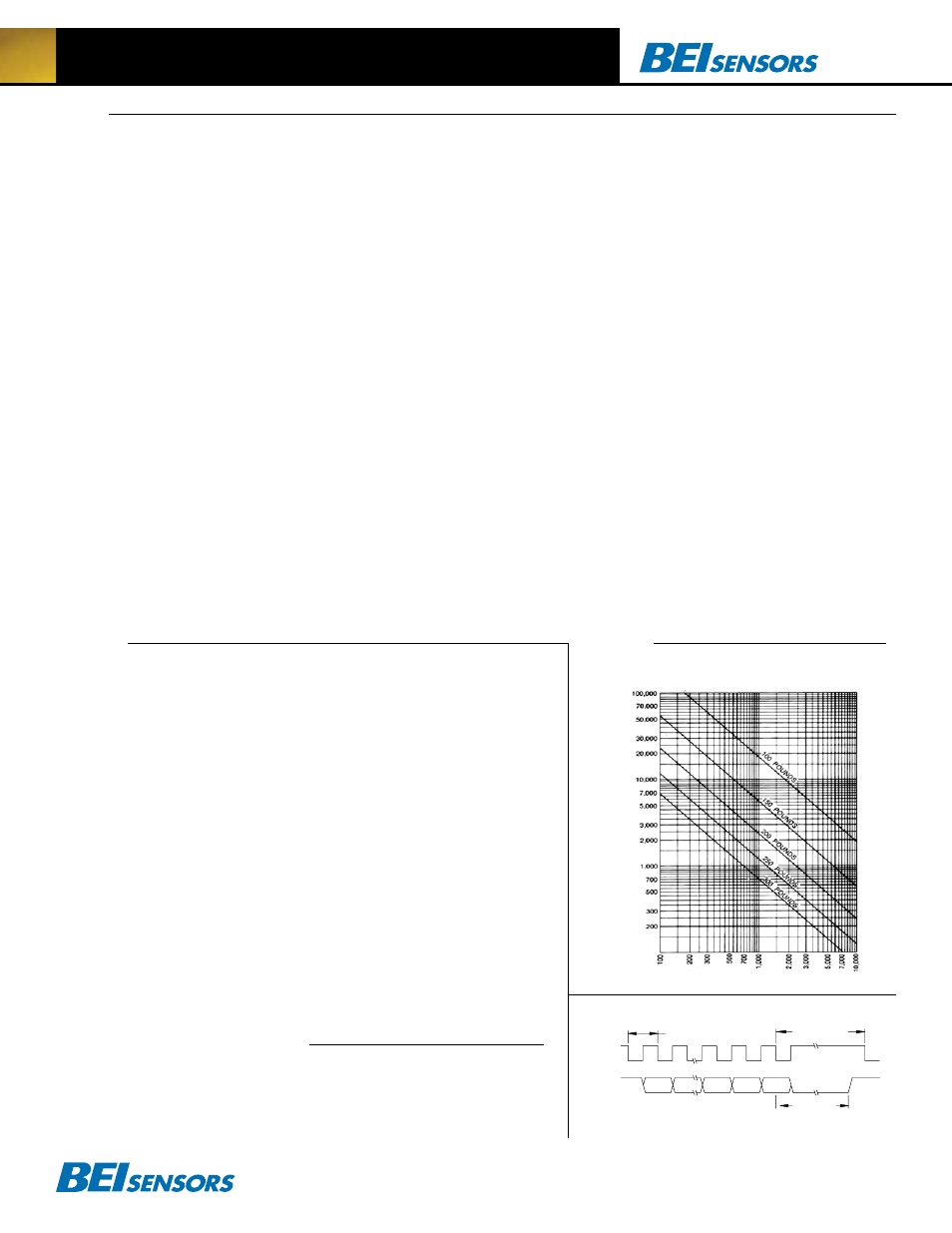
BEARING RATING LIFE (HOURS)
SPEED (RPM)
Bearing Life vs. Speed at Various Radial Loads
Serial Synchronous Interface (SSI)
SSI output provides effective synchronization in a closed-loop control
system. A clock pulse train from a controller is used to clock out sensor data: one bit of position data is transmitted to
the controller per one clock pulse received by the sensor. The use of a differential driver permits reliable transmission
of data over long distances in environments that may be electrically noisy. The encoder utilizes a clock signal, provided
by the user interface, to time the data transmission. Receiving electronics must include an appropriate receiver as well
as line terminating resistors.
Features :
•
Synchronous transmission
•
Transmission lengths to 1000 feet
•
Accepts clock rates from 100 KHz to 1.8 MHz
Data Transmission Sequence
1. Output driver of the encoder is a MAX 491 transceiver in
transmit mode. The recommended receiver is a MAX 491
transceiver in receive mode.
2. Controller provides a series of pulses (or differential
pulse pairs) on the CLOCK input lines.
3. On the first HIGH-to-LOW CLOCK transition, the encoder
latches its data at the current position and prepares to
transmit.
4. Controller reads data on the falling edge of the next 15
clock cycles.
5. The first bit is a START bit and is always HIGH.
6. Next comes 13 data bits beginning with the most sig-
nificant bit (MSB) and ending with the parity bit. On 12 bit
encoders, bit 13 is LOW. When parity is not ordered, parity
is LOW.
7. After the last CLOCK HIGH-to-LOW transition, a mini-
mum of 40 microseconds must pass before the beginning
of the next CLOCK series.
interfacing long Data lines
Cable impedance can create a transmission delay, in
effect, shifting the phase relationship between the clock
pulse and the data. If this phase shift exceeds 180°, then
the wrong bit position will be sampled by the receiver.
As a result, the maximum allowable clock frequency is
a function of the cable length. For 24 AWG, stranded, 3
pair cable (BEI part number 37048-003 or equivalent) the
group delay is 1.36ns/ft. The table below shows the maxi-
mum transmission rate allowable as a function of cable
length to ensure a phase shift of less than 90°.
Cable length (ft) 50 100 200 300 500 1000
Max Freq (kHz) 1800 900 500 300 200 100
CLOCK, Maximum (kHz) = 92,000 / Cable Length (ft)CW
7230 Hollister Avenue | Goleta, CA 93117-2891 | Tel: (805) 968-0782 | Fax: (805) 968-3154
0539
CONNECTOR*
DATA+
A
FUNCTION
YEL
CABLE
1
H40
TERM BOARD
DATA-
H
WHT/YEL
7
CLOCK+
B
BLU
2
CLOCK-
I
WHT/BLU
8
DIRECTION CONTROL
C
ORN
3
ENABLE (OPTIONAL)
J
WHT/ORN
9
SUPPLY VOLTAGE (+V)
D
RED
4
CIRCUIT COMMON (0V)
F
BLK
5
CASE GROUND
G
GRN
6
Max. Frequency (KHz)
Cable Length (feet)
50
1800
100
900
500
200
300
300
200
500
100
1000
1
2
12
13
14
15
START
BIT
MSB
MSB-1
LSB12
LSB13
Parity
(Optional)
DATA+
CLOCK+
START
BIT
NEXT CLOCK
START OF
4
2
1
3
9
6
8
7
5
H38
1RB90
A
SPECIFICATION ADDENDUM, Serial Synchronous Interface SSI):
SSI output provides effective synchronization in a closed-loop control system. A clock
pulse train from a controller is used to shift out sensor data: one bit of position data is
transmitted to the controller per clock pulse received by the sensor. The use of a
differential driver permits reliable transmission of data over long distances in
environments that may be electrically noisy. The encoder utilizes a clock signal,
provided by the user interface, to time the data transmission. Receiving electronics must
include an appropriate receiver as well as line terminating resistors. An optional parity
bit is available to validate the transmitted data.
Features:
Synchronous transmission
RS422/485 compatible
Transmission lengths to 1000 feet
Accepts clock rates from 100 KHz to 1.8 MHz
Parity bit option is available
Data Transmission
Sequence:
1. Data from the encoder is sent with a MAX 491 transceiver in transmit mode. It is
recommended to use any RS-422/485 compatible receiver and provide a termination resistor
based on the RS-422/485 specification for your specific voltage and DATA line length.
2. The CLOCK signals are RS-422/485 compatible, differential TTL, with 180 Ohm termination
resistors internal to the encoder. A series of pulses from the controller, on the CLOCK
lines, advances the data.
3. On the first HIGH-to-LOW CLOCK transition, the encoder latches its data at the current
position and prepares to transmit. The DATA signal during this transition is a START bit,
which is always HIGH.
4. The encoder shifts data to the DATA line on each LOW-to-HIGH clock transition, beginning
with the MSB. The controller reads data on the HIGH-to-LOW transiton of the next 12 clock
cycles ending with the LSB. The parity bit (if parity option is specified) is clocked out on
the 14th clock cycle. When the parity option is used, the 13th bit output is a logic LOW on
a 12 bit Encoder or the LSB of a 13 bit Encoder.
5. Parity is even. The sum of all data bits and the parity bit is even.
6. After the last CLOCK LOW-to-HIGH transition, a minimum of 30 microseconds must pass
before the beginning of the next CLOCK series.
SPECIFICATION ADDENDUM
Serial Synchronous Interface (SSI)
REVISIONS
DESCRIPTION
DIMENSIONS ARE IN INCHES
APPLY AFTER FINISH
REMOVE BURRS AND BREAK ALL
SHARP EDGES .010 MAX
ALL DIA. TO BE WITHIN .010
ANGLES ± 0 30'
.XXX ±.005
.XX ±.01
TOLERANCES ON
63
UNLESS OTHERWISE SPECIFIED
APPR
ENGR
CHECKED
SCALE: NONE
SIZE
A
TITLE
1RB90
FSCM NO.
KRB
redrawn
04/06/05
DATE
LTR
924-02087-001
DWG NO.
SHEET: 1/2
APPR
DATE
REV
A
924-02087-001
BEI
I N D U S T R I A L E N C O D E R D I V I S I O N
B E I T E C H N O L O G I E S , I N C.
BEI TECHNOLOGIES, INC. ANY REPRODUCTION, USE OR DISCLOSURE
THIS DOCUMENT CONTAINS PROPRIETARY INFORMATION OF
OF THIS DOCUMENT WITHOUT WRITTEN CONSENT OF
BEI TECHNOLOGIES, INC. IS EXPRESSLY PROHIBITED.
12-24VDC
(300mA MAX)
SIZE
FSCM NO.
SCALE: NONE
DWG NO.
A
SHEET: 2/2
BEI
I N D U S T R I A L E N C O D E R D I V I S I O N
B E I T E C H N O L O G I E S , I N C.
924-02087-001
REV
Interfacing Long Data Lines:
Cable impedance creates a transmission delay, shifting the phase relationship between the clock pulse and the data. If this pulse shift exceeds 180 , then the wrong bit position will be sampled
by the receiver. The maximum allowable clock frequency, therefore, is a function of the cable
length. For 24 AWG, stranded, 3 pair cable (BEI part number 37048-003 or equivalent) the group
delay is 1.36nS/ft. The table below shows the maximum transmission rate allowable as a function
of cable length to ensure a phase shift of less than 90 .
CLOCK: Maximum (KHz) = 92,000/Cable Length (ft)
*Connector is a MS3102E18-1P, 10-pin connector on the encoder body and mates to an MS3106F18-1S connector or can be used with a standard cable/connector assembly, BEI P/N: 924-31186-18XX.
(XX = cable length in feet, ie. 10 = 10 feet)
Direction Control: Standard is CW for increasing count when viewed from the shaft end. Direction Control (Pin C) is normally HIGH (or N/C) and is pulled up internally to the positive supply voltage. To reverse the count direction,
Pin C must be pulled to LO (0V)
SSI Compatible Serial Code (S3):
20us Max
SSI Compatible Output with Parity Option Timing Diagram:
40us Min
30us Min
Encoder:
H25D - SS - 12GC - S3 - SM18 - S
Example Model Number:
Specials:
-S = Parity Bit
To specify
SSI Output
A
ECO_500
4/13/05
30
40
SSi Timing