Communication Concepts AN762 Application Note User Manual
Page 7
AR
C
HIVE INF
O
RMA
TI
O
N
PRODUCT TRANSFERRED T
O
M/A
–
COM
AN762
7
RF Application Reports
This number can be used to select a suitable heat sink
for the amplifier. The information is given by most
manufacturers for their standard heat sinks, or specific
lengths of extrusion. As an example, a 9.1
″ length of
thermalloy 6153 or a 7.6
″ length of Aavid Engineering 60140
extrusion would be required for 100% duty cycle, unless the
air velocity is increased by a fan or other means.
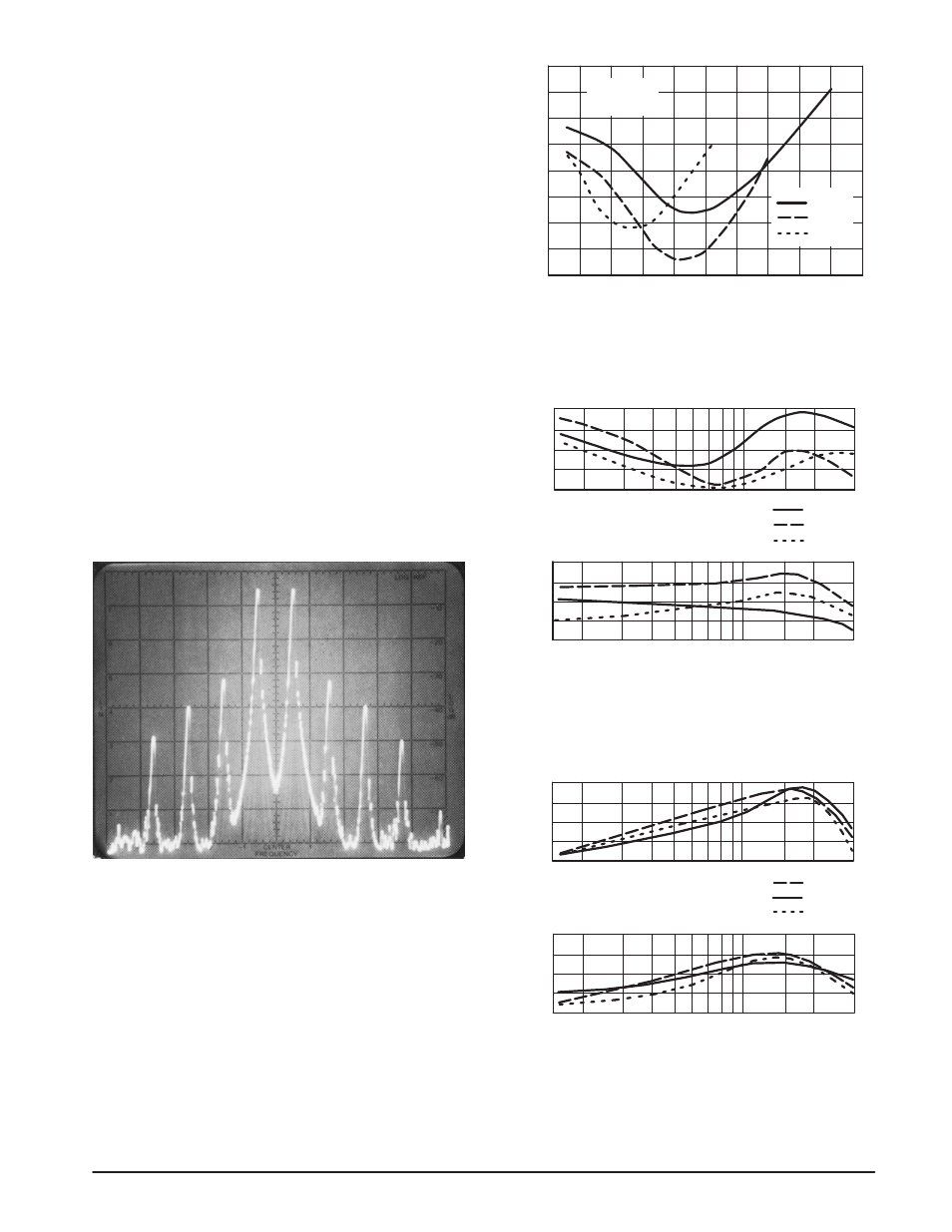
PERFORMANCE AND MEASUREMENTS
The performance of each amplifier was measured with
equipment similar to what is described in reference
(2)
. The
solid lines in Figures 6, 7, 8 and 9 represent the 100 W unit,
the dashed lines represent the 140 W unit, and the dotted
lines refer to the 180 W version. The data presented is
typical, and spreads in the transistor h
FE
’s will result in slight
variations in RF power gain (Figure 7).
The performance data is also affected by the purity of the
driving source. There should be at least 5 – 6 dB IMD margin
to the expected power amplifier specification, and a harmonic
suppression of 50 dB minimum below the fundamental is
recommended
(7)
.
The IMD measurements were done in accordance to the
E.l.A. proposed standard, commonly employed in Ham Radio
and other commercial equipment design. The distortion
products are referenced to the peak power, and adjusting
the tone peaks 6 dB below the 0 dB line on the spectrum
analyzer screen (Figure 5) provides a direct reading on the
scale.
Figure 5. An Example of the IMD Spectral Display
(c. Power Output = 180 W PEP, 30.00 MHz)
The Two Tones Have Been Adjusted 6 dB Below the Top
Line, and the Distortion Products Relative to Peak Power
can be Directly Read on the Scale.
The collector efficiency under two tone test condtions is
normally 15 – 20% lower than at CW. The load line has been
optimized for the peak power (as well as possible in a
broadband system with transformer impedance ratios of 4:1,
9:1, 16:1, 25:1, etc. available), which at SSB represents a
smaller duty cycle, and the power output varies between zero
and maximum. Typical figures are 40 – 45% and 55 – 65%
respectively.
POWER OUTPUT (WATTS, PEP)
IMD (dB)
- 30
0
40
80
120
160
200
- 35
- 40
- 45
- 50
180 W
140 W
100 W
c
a
b
f = 30.0 MHz
V
CC
= 13.6 V
Figure 6. Intermodulation Distortion versus
Power Output
FREQUENCY (MHz)
INTERMODULA
TION
- 30
1.5 2.0
3.0
5.0
10
30
- 35
- 40
16
15
180 W
140 W
100 W
V
CC
= 13.6 V
14
13
12
7.0
15
20
a
c
b
a
c
b
POWER GAIN (dB)
DIST
OR
TION (dB)
Figure 7. IMD and Power Gain versus Frequency
FREQUENCY (MHz)
COLLECT
OR EFFICIENC
Y
50
1.5 2.0
3.0
5.0
10
30
45
40
2.00
180 W
140 W
100 W
V
CC
= 13.6 V (TWO TONE TEST)
1.50
1.00
7.0
15
20
a
c
b
a
c
b
INPUT
VSWR
(%)
Figure 8. Input VSWR and Collector Efficiency
versus Frequency