Archive informa tion archive informa tion – Communication Concepts EB104 Engineering Bulletin User Manual
Page 5
ARCHIVE INFORMA
TION
ARCHIVE INFORMA
TION
EB104
5
RF Application Reports
- 25
- 30
- 20
- 35
- 40
- 45
I
DQ
= 4 x 250 mA
100
200
300
400
500
600
0
40 V
50 V
2.0 MHz
30 MHz
40 V
50 V
POWER OUTPUT (WATTS, PEP)
- 25
- 30
- 20
- 35
- 40
- 45
3RD ORDER IMD (dB)
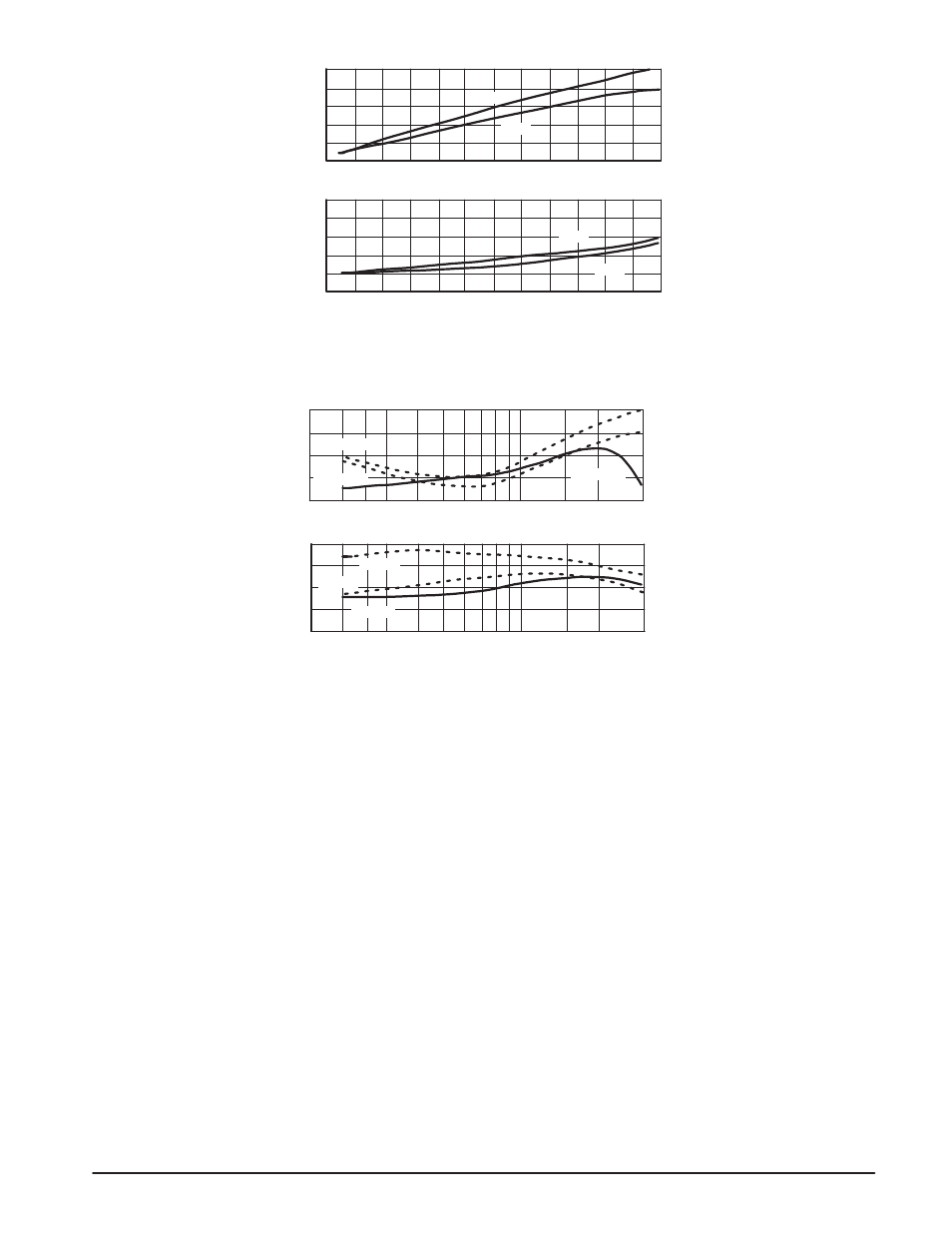
Figure 6.
FREQUENCY (MHz)
60
50
η
40 V
INPUT
VSWR
VSWR
P
out
= 600 W, I
DQ
= 4 x 250 mA
IMD (d ) BELOW
3
ONE
TONE
40
40
30
20
CW DRAIN
EFFICIENCY
(%)
2.0
4.0
7.0
10
15
30
22
21
20
2.0
1.5
1.0
POWER GAIN (dB)
IMD 40 V
IMD 50 V
GPS 50 V
η
50 V
Figure 7.
and as can be expected with FETs, the 9th and higher order
products are in the – 50 to – 60 dB level. It can also be no-
ticed from Figure 6, that the IMD does not increase at re-
duced power levels, as common with bipolar amplifiers. The
even order output harmonic content depends greatly on the
device balance as in any push-pull circuit. The worst case is
at the low frequencies, where numbers like – 30 to – 40 dB
for the 2nd harmonic is typical. The highest 3rd harmonic
amplitude of – 12 dB is at 6.0 – 8.0 MHz carrier frequency.
Information on suitable harmonic filters is available in Refer-
ence 3. The stability of the amplifier has been tested into a
3:1 load mismatch at all phase angles. It was found to be
completely stable, even at reduced supply voltages. In a
MOSFET (common source) the ratio of feedback capaci-
tance to the input impedance is several times higher than
that of a bipolar transistor (common emitter). As a result, a
properly designed FET circuit should be inherently more
stable, especially under varying load conditions.
It must be noted, that special attention must be given to
the heat sink design for this unit. With the 200 – 300 watts
of heat generated by the transistors in a small physical area,
it must be conducted into a heat sink efficiently. This can
only be done with high conductance material, such as
copper. If aluminum heat sink is used, a copper heat
spreader is recommended between the transistor flanges
and the heat sink surface.