Archive informa tion archive informa tion – Communication Concepts EB104 Engineering Bulletin User Manual
Page 2
ARCHIVE INFORMA
TION
ARCHIVE INFORMA
TION
EB104
2
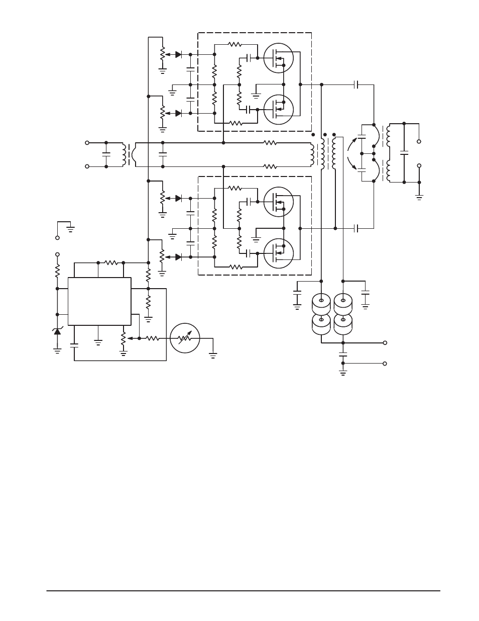
RF Application Reports
R1 – R5 — 10 k Trimpot
R6 — 1.0 k/1.0W
R7 — 10 Ohms
R8 — 2.0 k
R9, R21, R22, R23, R24 — 10 k
R10 — 8.2 k
R11, R12, R13, R14 — 100 Ohms
R15, R16, R17, R18 — 2.7 Ohms
R19, R20 — 10 Ohms/2.0 W Carbon
R25 — Thermistor, 10 k (25
°
C), 2.5 k (75
°
C)
C1 — Not used
C2 — 820 pF Ceramic chip
C3, C4, C5, C6, C13, C14 — 0.1
µ
F Ceramic
C7, C8, C9, C10 — 0.1
µ
F Ceramic chip
C11 — 1200 pF each, 680 pF mica in parallel with an
Arco 469 variable or three or more smaller value
mica capacitors in parallel
C12 — Not used
C15 — 10
µ
F, 100 V Electrolytic
C16 — 1000 pF Ceramic
C17, C18 — Two 0.1
µ
F, 100 V Ceramic each, (ATC 200/823 or
equivalent)
D1, D2, D3, D4 — 1N4148
D5 — 28 V Zener, 1N5362 or equivalent
B1, B2, B3, B4 — Ferrite Beads
L1, L2 — Two Fair-Rite 2673021801 ferrite beads each or equivalent,
4.0
µ
H
T1, T2, T3 — See text
Q1, Q2, Q3, Q4 — MRF150
IC1 — MC1723CP
All resistors 1/2 W carbon or metal film unless otherwise
designated.
+
V
DS
-
R1
R11
C17
Q1
C7
C1
T1
INPUT
C13
L1
C15
C4
C18
T2
+
-
OUTPUT
L2
C14
T3
C16
R9
R7
R5
R10
R25
R8
3
10
2
12
11
13
7
6
5
4
IC1
C12
R15
R21
R16
R22
C8
R12
R19
R20
Q2
C3
D2
D1
R2
D5
R3
R13
Q3
C9
C6
R17
R23
R18
R24
C10
R14
Q4
C5
D4
D3
R4
R6
BIAS
C2
C11
Figure 2. Detailed Schematic