Pulse pattern and data functionality, Jitter emulation (delay control input), Data generation – Atec Agilent-81133A-81134A User Manual
Page 7: Prbs 2, Trigger output, Delay control input

6
7
Pulse Pattern and Data Functionality
The 81133A and 81134A can generate an 8 KBit digital
pattern in NRZ, RZ and R1 mode. Furthermore, the 81133A
and 81134A can provide a hardware generated pseudo
random binary sequence (PRBS) from 2
5
- 1 to 2
31
- 1.
Jitter Emulation (Delay Control Input)
Full control over the signal quality of pulse and data
signals provides the Delay Control Input. With an external
modulation source (e.g. Agilent 33250A) the amount and
shape of signal jitter can be varied for stress tests or to
emulate real world signals. The external source for jitter
modulation is applied to this input. Jitter modulation can
be turned on and off individually for each channel. Either
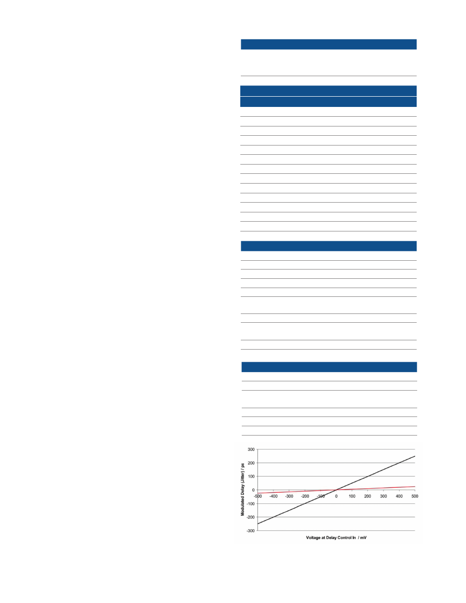
one of two fixed sensitivities can be selected ± 25 ps or
± 250 ps resulting in a total of 50 ps or 500 ps. The ampli-
tude of the modulated jitter is set by the voltage level of
the signal applied to the Delay Control Input. The Variable
Crossover Point feature provides additional control over
the signal quality.
Data generation
Memory depth
8 Kbit per channel/12 Mbit extended
memory
Data format
RZ/NRZ/R1
PRBS 2
n
-1 , n = 5, 6, 7, 8, 9, 10, 11, 12, 13, 14, 15, 23, 31
PRBS Polynomial
Comment
2
5
-1
X
5
+ X
4
+ X
2
+ X
1
+ 1
2
6
-1
X
6
+ X
5
+ X
3
+ X
2
+ 1
ITU-T V.29
2
7
-1
X
7
+ X
6
+ 1
2
8
-1
X
8
+ X
7
+ X
3
+ X
2
+ 1
2
9
-1
X
9
+ X
5
+ 1
CCITT 0.153/ITU-T V.52
2
10
-1
X
10
+ X
7
+ 1
CCITT 0.152/ITU-T 0.152
2
11
-1
X
11
+ X
19
+ 1
2
12
-1
X
12
+ X
9
+ X
8
+ X
5
+ 1
2
13
-1
X
13
+ X
12
+ X
10
+ X
9
+ 1
2
14
-1
X
14
+ X
13
+ X
10
+ X
9
+ 1
2
15
-1
X
15
+ X
14
+ 1
CCITT 0.151/ITU-T 0.151
2
23
-1
X
23
+ X
18
+ 1
CCITT 0.151/ITU-T 0.151
2
31
-1
X
31
+ X
28
+ 1
Trigger output
Amplitude
50 mV to 2.00 V
Level window
–2.00 V . . +3.00 V
Resolution
10 mV
Format fixed duty cycle,
50% nominal
Maximum external voltage
–2.00 V . . +3.00 V
Transition times
(20% to 80% of amplitude)
< 100 ps (< 70 ps typical)
Minimum output frequency
15 MHz/divider factor
Mode clock clock divided
by 1,2,3, . .
2
31
-1 or trigger on bit 0 of data
Disable
Yes (relay)
Delay control input
Interface
dc-coupled
Impedance
50 Ohm nominal
Input levels for full modulation
range
±500 mV
Max input levels
±2.5 V
Delay modulation range
±250 ps, ±25 ps, selectable
Modulation frequency
0 Hz - 200 MHz
Figure 2. Modulated Delay (Jitter) vs Voltage Level at
Delay-Control-Input for ±250 ps and ±25 ps settings
