6 system startup – Alpha Technologies CXPS-HD 48-1.2-225 User Manual
Page 30
0530082-J0 Rev B
Page 22 of 31
6 System
startup
After completing the system installation and power system wiring, perform the following:
6.1
Check system connections
x Ensure that the AC input is switched off, the battery breaker is off, and all power modules are removed from
the shelf.
x Triple-check the polarity of all the connections.
6.2
Verify AC input and power up rectifier shelf
1. Install one rectifier module.
2. Verify that the AC input voltage is correct and switch on the corresponding feeder breaker.
3. The controller OK LED light should illuminate continuously after a preset start delay.
4. Using the controller, test the functionality of all module alarms and controls.
6.3
Check battery polarity and connect the batteries
1. Verify the polarity of all the batteries with a voltmeter to ensure that no cells or batteries are reversed.
2. Switch on the appropriate battery breaker.
3. Install the remaining power modules.
4. Use a web browser to access the adjustments menu of the controller. Set the float and equalize the voltage to
the levels specified by the battery manufacturer.
5. Using the controller, test the functionality of various module alarms and controls. In addition, perform a load
test with the system using a resistive load box if needed.
6. Enable the temperature compensation (Temp Comp) feature on the Batteries menu. Program the slope
setting and the upper and lower breakpoints according to the specific battery requirements.
6.3.1
Controller alarm configuration for nominal 120 Vac operation
The default setting for the low AC input alarm is 180 Vac. For a nominal 120 Vac input, reset this value to
100 Vac.
1. Select
Alarms > Configure Alarms. Under Alarm Configuration, select Voltage Alarms.
2. Select and modify the activation value for AC Mains Low to 100 Vac.
3. Submit the changes to save the new configuration.
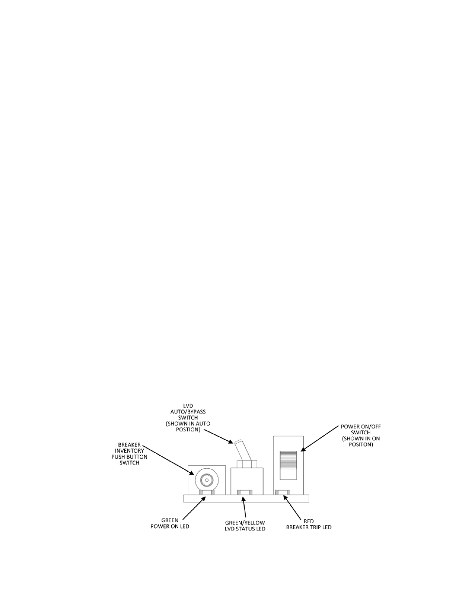
6.3.2
Setup and operation of the distribution panel
Figure 8–Layout and Function of Switches on Front of Logic PCB