Dmg1016udw new prod uc t, Electrical characteristics p-channel – q2, Dmg1016udw – Diodes DMG1016UDW User Manual
Page 5
DMG1016UDW
Document number: DS31860 Rev. 6 - 2
5 of 9
January 2014
© Diodes Incorporated
DMG1016UDW
NEW PROD
UC
T
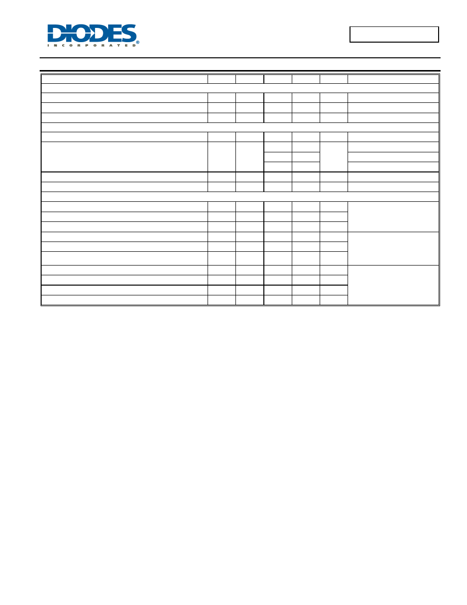
Electrical Characteristics P-CHANNEL – Q2
(@T
A
= +25°C, unless otherwise specified.)
Characteristic
Symbol
Min
Typ
Max
Unit
Test Condition
OFF CHARACTERISTICS (Note 6)
Drain-Source Breakdown Voltage
BV
DSS
-20
— — V
V
GS
= 0V, I
D
= -250μA
Zero Gate Voltage Drain Current @T
c
= +25°C
I
DSS
— — -100 nA
V
DS
= -20V, V
GS
= 0V
Gate-Source Leakage
I
GSS
— — ±2.0
μA
V
GS
= ±4.5V, V
DS
= 0V
ON CHARACTERISTICS (Note 6)
Gate Threshold Voltage
V
GS(th)
-0.5 — -1.0 V
V
DS
= V
GS
, I
D
= -250μA
Static Drain-Source On-Resistance
R
DS (ON)
—
0.5 0.75
Ω
V
GS
= -4.5V, I
D
= -430mA
0.7 1.05
V
GS
= -2.5V, I
D
= -300mA
1.0 1.5
V
GS
= -1.8V, I
D
= -150mA
Forward Transfer Admittance
|Y
fs
|
—
0.9 — S
V
DS
= -10V, I
D
= -250mA
Diode Forward Voltage (Note 6)
V
SD
—
-0.8 -1.2 V
V
GS
= 0V, I
S
= -150mA
DYNAMIC CHARACTERISTICS (Note 7)
Input Capacitance
C
iss
—
59.76
—
pF
V
DS
= -16V, V
GS
= 0V,
f = 1.0MHz
Output Capacitance
C
oss
—
12.07
—
pF
Reverse Transfer Capacitance
C
rss
—
6.36
—
pF
Total Gate Charge (4.5V)
Q
g
—
622.4
—
pC
V
GS
= -4.5V, V
DS
= -10V,
I
D
= -250mA
Gate-Source Charge
Q
gs
—
100.3
—
pC
Gate-Drain Charge
Q
gd
—
132.2
—
pC
Turn-On Delay Time
t
D(on)
—
5.1
—
ns
V
DS
= -10V, V
GS
= -4.5V,
R
G
= 10Ω, R
L
= 47Ω
Turn-On Rise Time
t
r
—
8.1
—
ns
Turn-Off Delay Time
t
D(off)
—
28.4
—
ns
Turn-Off Fall Time
t
f
—
20.72
—
ns
Notes:
6. Short duration pulse test used to minimize self-heating effect.
7. Guaranteed by design. Not subject to production testing