Preliminary datasheet, Recommended operating conditions – Diodes AZV831/2 User Manual
Page 5
Preliminary Datasheet
Single/Dual Low Bias Current, Low Voltage, Rail-to-Rail
Input/Output CMOS Operational Amplifiers
Jul. 2012 Rev. 1. 0 BCD Semiconductor Manufacturing Limited
5
AZV831/2
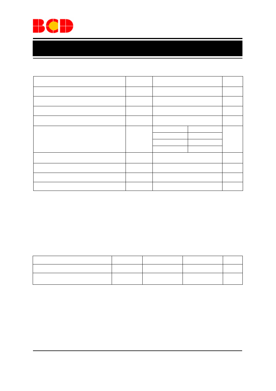
Absolute Maximum Ratings (Note 1)
Parameter Symbol
Value
Unit
Power Supply Voltage
V
CC
6.0 V
Differential Input Voltage
V
ID
6.0 V
Input Voltage
V
IN
-0.3
to
V
CC
+0.5 V
Operating Junction Temperature
T
J
150
ºC
Thermal Resistance
(Junction to Ambient)
θ
JA
SC-70-5 270
ºC /W
SOT-23-5 220
SOIC-8 150
MSOP-8 200
Storage Temperature Range
T
STG
-65
to
150 ºC
Lead Temperature (Soldering,10 Seconds)
T
LEAD
260 ºC
ESD (Human Body Model)
4000
V
ESD (Machine Model)
300
V
Note 1: Stresses greater than those listed under “Absolute Maximum Ratings” may cause permanent damage to
the device. These are stress ratings only, and functional operation of the device at these or any other conditions
beyond those indicated under “Recommended Operating Conditions” is not implied. Exposure to “Absolute
Maximum Ratings” for extended periods may affect device reliability.
Recommended Operating Conditions
Parameter
Symbol Min
Max Unit
Supply Voltage
V
CC
1.6
5.5
V
Operation Ambient Temperature
Range
T
A
-40 85
ºC