Preliminary datasheet, With resistive load with capacitive load – Diodes AZV831/2 User Manual
Page 14
Preliminary Datasheet
Single/Dual Low Bias Current, Low Voltage, Rail-to-Rail
Input/Output CMOS Operational Amplifiers
Jul. 2012 Rev. 1. 0 BCD Semiconductor Manufacturing Limited
14
AZV831/2
Typical Performance Characteristics (Continued)
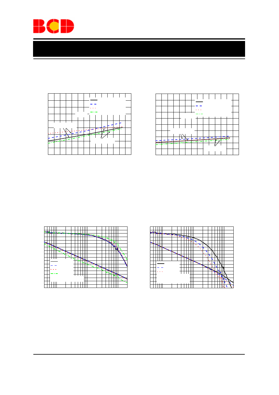
Figure 20. Output Voltage Swing vs. Temperature Figure 21. Output Voltage Swing vs. Temperature
Figure 22. Gain and Phase vs. Frequency Figure 23. Gain and Phase vs. Frequency
with Resistive Load with Capacitive Load
-40
-20
0
20
40
60
80
100
12
16
20
24
28
32
36
40
44
48
Negative Swing
R
L
=1k
Ω
Out
pu
t Vol
tage t
o Supply
Rai
l (
m
V)
Temperature (
o
C)
V
CC
=0.8V,V
EE
=-0.8V
V
CC
=2.5V,V
EE
=-2.5V
V
CC
=0.8V,V
EE
=-0.8V
V
CC
=2.5V,V
EE
=-2.5V
Positive Swing
-40
-20
0
20
40
60
80
100
0
1
2
3
4
5
6
7
8
9
10
Positive Swing
R
L
=10k
Ω
V
CC
=0.9V,V
EE
=-0.9V
V
CC
=1.5V,V
EE
=-1.5V
V
CC
=0.9V,V
EE
=-0.9V
V
CC
=1.5V,V
EE
=-1.5V
O
u
tput Voltage to Suppl
y
Rail
(m
V
)
Temperature (
o
C)
Negative Swing
10k
100k
1M
-20
-10
0
10
20
30
40
50
60
70
10
20
30
40
50
60
70
80
90
100
V
CC
=0.8V, V
EE
=-0.8V
O
pen
Lo
op
G
ai
n (dB)
Frequency (Hz)
R
L
=100k
Ω
R
L
=10k
Ω
R
L
=1k
Ω
R
L
=8
Ω
Phase M
argi
n (
D
egree)
10k
100k
1M
-20
-10
0
10
20
30
40
50
60
70
10
20
30
40
50
60
70
80
90
100
V
CC
=0.8V, V
EE
=-0.8V
R
L
=100k
Ω
O
pen
Lo
op
G
ai
n (dB)
Frequency (Hz)
C
L
=100pF
C
L
=200pF
C
L
=300pF
Phase M
argi
n (
D
egree)