Design formula table, Al8812 – Diodes AL8812 User Manual
Page 9
AL8812
Document number: DS37099 Rev. 1 - 2
9 of 11
March 2014
© Diodes Incorporated
AL8812
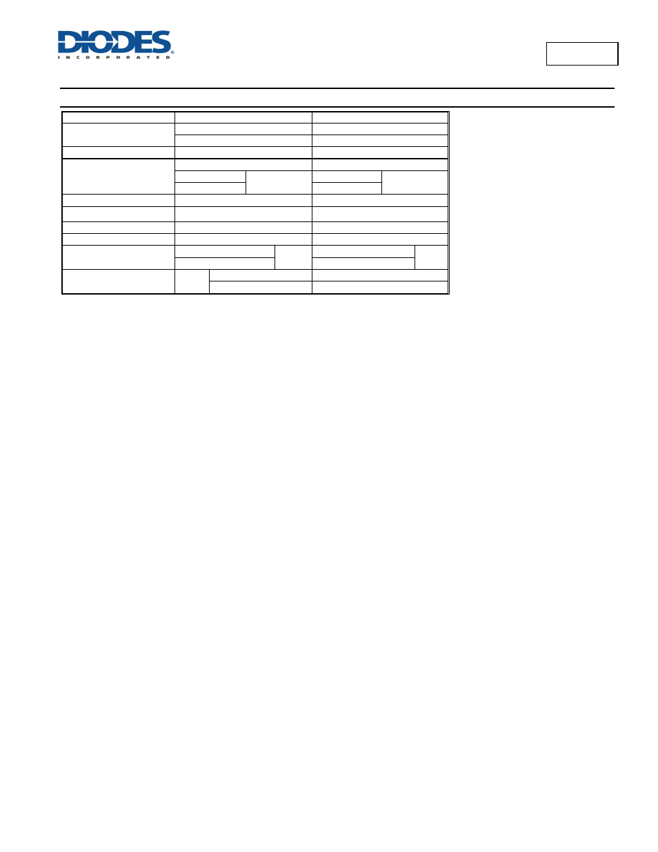
Design Formula Table
Calculation
Boost
Buck
t
ON
/ t
off
V
OUT
+ V
F
-V
IN (min)
V
OUT
+ v
F
V
IN (min)
- V
sat
V
IN (min)
- V
SAT
- V
OUT
( t
ON
+ t
off
)
1/f
1/f
t
off
t
ON
+ t
OFF
t
ON
+ t
OFF
t
ON
+1
t
ON
+1
t
OFF
t
OFF
t
ON
( t
ON
+t
OFF
) - t
OFF
( t
ON
+t
OFF
) - t
OFF
C
T
4.0
×10
-5
t
ON
4.0
×10
-5
t
ON
I
pk
(switch)
2I
OUT (max)
(t
ON
/ t
off
+1)
2I
OUT (max)
R
sc
0.3 / I
pk (switch)
0.3 / I
pk (switch)
L
(min)
( V
IN (min)
– V
sat
)
t
on (max)
( V
IN (min)
– V
SAT
-V
OUT
)
ON (max)
I
pk (switch)
I
pk (switch)
C
O
9
I
OUT
t
ON
I
pk (switch)
( t
OFF
+ t
ON
)
V
ripple (pp)
8V
ripple (pp)
V
sat
= Saturation voltage of the output switch.
V
F
= Forward voltage drop of the output rectifier.
The following power supply characteristics must be chosen:
V
IN
- Nominal input voltage.
V
OUT
- Desired output voltage, |V
OUT
| = 1.25 (1+R2/R1)
I
OUT
- Desired output current.
f
min
- Minimum desired output switching frequency at the selected values of V
in
and I
o
.
V
ripple(pp)
- Desired peak-to-peak output ripple voltage. In practice, the calculated capacitor value will need to be increased due to its
equivalent series resistance and board layout. The ripple voltage should be kept to a low value since it will directly affect the line and
load regulation.