Al8812, Pin descriptions, Functional diagram – Diodes AL8812 User Manual
Page 2
AL8812
Document number: DS37099 Rev. 1 - 2
2 of 11
March 2014
© Diodes Incorporated
AL8812
Pin Descriptions
Pin
Name
Pin
Number
(U-DFN6040-12)
Function
NC 1
No
Connection
GATE
2
Gate connection of internal MOSFET.
INPUT
3
Feedback pin for inverting input of internal comparator
VCC
4
Supply voltage pin
SENSE 5
No
Connection.
DRIVE 6
Current drive collector:
Normally connected to V
CC
directly or via a resistor.
SW/C
7
Internal switch transistor collector
SW/E
8
Internal switch transistor emitter
GND 9
Ground
Connection
TIMING
10
Timing Capacitor to control the switching frequency.
SOURCE
11
Source connecton of internal MOSFET
DRAIN
12
Drain connection of internal MOSFET
Exposed PAD1
Exposed Pad of MOSFET Drain
Exposed PAD2
Exposed Pad of AL8812 and connect to PCB ground
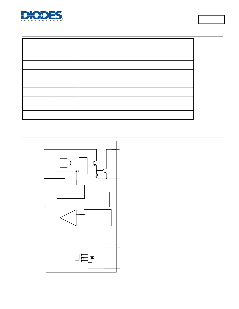
Functional Diagram
1.25V
Reference
Regulator
Ipk
Oscillator
C
T
R
S
Q
Q2
Q1
100
Comparator
+
_
GND
TIMING
SW/E
SW/C
D
RIVE
SENSE
VCC
INPUT
GATE
DRAIN
SOURCE
2
3
4
5
6
7
8
9
10
12
11