Absolute maximum ratings, Electrical characteristics, Al8812 – Diodes AL8812 User Manual
Page 3
AL8812
Document number: DS37099 Rev. 1 - 2
3 of 11
March 2014
© Diodes Incorporated
AL8812
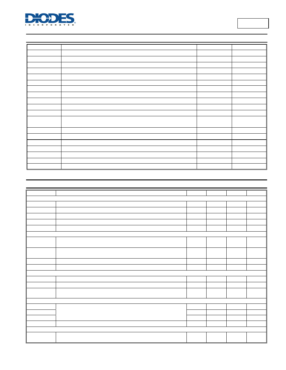
Absolute Maximum Ratings
(@T
A
= +25°C, unless otherwise specified.)
Symbol
Parameter
Value
Unit
V
CC
Power Supply Voltage
20
V
V
IR
Comparator Input Voltage Range
-0.3 to +36
V
SW/C
Switch Collector Voltage
36
V
SW/E
Switch Emitter Voltage (V
Pin
1 = 40V)
36
V
V
CE (switch)
Switch Collector to Emitter Voltage
36
V
DRIVE
Driver Collector Voltage
36
V
I
C (driver)
Driver Collector Current (Note 4)
100
mA
I
SW
Switch Current
1.6
A
V
DS
Maximum MOSFET Drain-Source voltage
60
V
V
GS
Maximum MOSFET Gate-Source voltage
+/-20
V
I
SOURCE
Maximum Continuous Source (Body Diode) Current
3.7
A
P
D
Continuous Power Dissipation (T
A
= +25
°C)
(U-DFN6040-12 (derate 10mW/
°C above +25°C)
1000
mW
θ
JA
Junction-to-Ambient Thermal Resistance
47.31
°C/W
θ
JC
Junction-to-Case Thermal Resistance
6.42
°C/W
T
MJ
Maximum Junction Temperature
+150
°C
T
OP
Operating Junction Temperature Range
0 to +105
°C
T
stg
Storage Temperature Range
-65 to +150
°C
ESD HBM
Human Body Model ESD Protection
250
V
ESD MM
Machine Model ESD Protection
100
V
Note:
4. Maximum package power dissipation limits must be observed.
Electrical Characteristics
(@T
A
= +25°C, unless otherwise specified.)
Symbol
Characteristics
Min
Typ
Max
Unit
OSCILLATOR
f
osc
Frequency (V
PIN
5 = 0V, C
T
= 1.0nF, T
A
= +25
°C)
24
33
42
kHz
I
chg
Charge Current (V
CC
= 5.0V to 40V, T
A
= +25
°C)
24
30
42
μA
I
dischg
Discharge Current (V
CC
= 5.0V to 40V, T
A
= +25
°C)
140
200
260
μA
I
dischg
/ I
chg
Discharge to Charge Current Ratio (Pin 7 to V
CC
, T
A
= +25
°C)
5.2
6.5
7.5
—
V
ipk (sense)
Current Limit Sense Voltage (I
chg
= I
dischg
, T
A
= +25
°C)
300
400
450
mV
OUTPUT SWITCH (Note 5)
V
CE (sat)
Saturation Voltage, Darlington Connection
(I
SW
= 1.0A, Pins 1,8 connected)
—
1.0
1.3
V
V
CE (sat)
Saturation Voltage, Darlington Connection
(I
SW
= 1.0A, ID = 50mA, Forced ß ≈ 20)
—
0.45
0.7
V
h
FE
DC Current Gain (I
SW
= 1.0A, V
CE
= 5.0V, T
A
= +25
°C)
50
75
—
—
I
C (off)
Collector Off-State Current (V
CE
= 40V)
-
0.01
100
μA
OUTPUT MOSFET
V
GS(th)
MOSFET Gate Threshold voltage
1
—
2.2
V
V
FD
MOSFET Diodes forward voltage
—
.85
.95
V
R
DS(ON)
Drain-source on-resistance (VGS = 10V, ID = 2.5A)
Drain-source on-resistance (VGS = 4.5V, ID = 2A)
—
—
120
180
mΩ
mΩ
COMPARATOR
V
th
Threshold Voltage
T
A
= +25
°C
T
A
= 0
o
C to +70
o
C
—
—
—
V
—
1.225
1.25
1.275
—
—
1.21
—
1.29
—
Reg
line
Threshold Voltage Line Regulation (V
CC
= 3.0V to 40V)
—
1.4
6.0
mV
TOTAL DEVICE
I
CC
Supply Current (V
CC
= 5.0V to 40V, C
T
=1.0nF, Pin 7 = V
CC
, V
Pin 5
> V
th
Pin 2
= Gnd, remaining pins open)
—
—
3.5
mA
Note:
5. Low duty cycle pulse techniques are used during test to maintain junction temperature as close to ambient temperature as possible.