Diodes AP2210 User Manual
Page 20
300mA RF ULDO REGULATOR AP2210
Data Sheet
20
Jan. 2012 Rev. 1. 6
BCD Semiconductor Manufacturing Limited
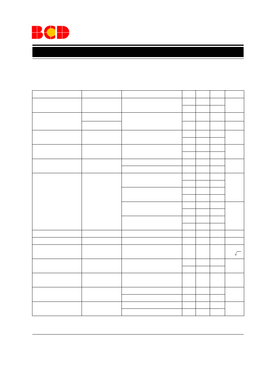
Parameter
Symbol
Conditions
Min
Typ
Max
Unit
Output Voltage Accuracy
∆V
OUT
/V
OUT
Variation from specified
V
OUT
-1
1
%
-2
2
Output Voltage
Temperature Coefficient
(Note 3)
∆V
OUT
/
∆T
120
µV/
o
C
(
∆V
OUT
/V
OUT
)/
∆T
48
ppm/
o
C
Line Regulation
V
RLINE
V
IN
=V
OUT
+1V to 13.2V
1.5
4.5
mV
12
Load Regulation
(Note 4)
V
RLOAD
I
OUT
=0.1mA to 300mA
1
6
mV
30
Standby Current
I
STD
V
EN
≤0.4V (shutdown)
0.01
1
µA
V
EN
≤0.18V (shutdown)
5
Ground Pin Current
(Note 6)
I
GND
V
EN
≥2.0V, I
OUT
=100
µA
100
150
µA
180
V
EN
≥2.0V, I
OUT
=50mA
350
600
800
V
EN
≥2.0V, I
OUT
=150mA
1.3
1.9
mA
2.5
V
EN
≥2.0V, I
OUT
=300mA
4
10
15
Ripple Rejection
PSRR
f=100Hz, I
OUT
=100
µA
75
dB
Current Limit
I
LIMIT
V
OUT
=0V
450
900
mA
Output Noise
e
no
I
OUT
=50mA, C
OUT
=2.2
µF,
100pF from BYP to GND
260
Enable Input Logic-low
Voltage
V
IL
Regulator shutdown
0.4
V
0.18
Enable Input Logic-high
Voltage
V
IH
Regulator enabled
2.0
V
Enable Input Logic-low
Current
I
IL
V
IL
≤0.4V
0.01
1
µA
V
IL
≤0.18V
2
Enable Input Logic-high
Current
I
IH
V
IL
≥2.0V
5
20
µA
V
IL
≥2.0V
25
Hz
nV /
V
IN
=V
OUT
+1V, I
OUT
=100
µA, C
IN
=1.0
µF, C
OUT
=2.2
µF, V
EN
≥2.0V, T
J
=25
o
C, Bold typeface applies over -40
o
C
≤T
J
≤125
o
C
(Note 2), unless otherwise specified.
Electrical Characteristics (Continued)
AP2210-ADJ Electrical Characteristics