Ap3105na/nv/nl/nr, Electrical characteristics – Diodes AP3105NA/NV/NL/NR User Manual
Page 5
AP3105NA/NV/NL/NR
Document number: DS36542 Rev. 1 - 2
5 of 13
www.diodes.com
September 2013
© Diodes Incorporated
AP3105NA/NV/NL/NR
A Product Line of
Diodes Incorporated
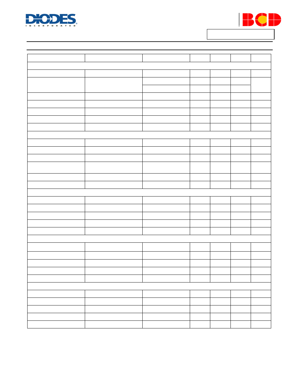
Electrical Characteristics
(@T
A
= +25°C, V
CC
= 16V, unless otherwise specified.)
Symbol Parameter
Conditions
Min
Typ
Max
Unit
Supply Voltage (VCC Pin)
I
STARTUP
Startup Current
–
2
5
20
μA
I
CC
Operating Supply Current
V
FB
=0V, C
L
=1nF
0.5 0.85 1.2
mA
V
FB
=3V, C
L
=0nF
0.6 1.2 2.0
–
U
VLO (on)
–
14.5 15.5 16.5 V
–
V
CC
Maintain
–
9.7 10.2 10.7 V
–
U
VLO
(off)
–
7.6 8.6 9.6 V
–
V
CC
OVP
–
27 28.5 30 V
–
V
CC
Clamp
I
CC
=5mA
31 34 – V
PWM Section/Oscillator Section
–
Maximum Duty Cycle
–
70 75 80 %
–
Oscillation Frequency
–
60 65 70 kHz
–
Green Mode Frequency
–
20
–
30 kHz
–
Frequency Temperature
Stability
-20
o
C to 125
o
C (Note 2)
–
–
5 %
–
Frequency Voltage Stability
V
CC
=12V to 30V
–
–
3 %
–
Frequency Dithering
–
±4
±6
±8
%
Current Sense Section (SENSE Pin)
V
CS
Maximum SENSE Voltage
V
FB
=3.6V
0.9 0.95 1 V
–
FOCP Voltage
–
1.65 1.8 1.95 V
–
LEB Time of SENSE
–
150 250 350 ns
–
Delay to Output (Note 2)
–
– 100 – ns
–
Soft-start Time
–
3 5 8 ms
Feedback Input Section (FB Pin)
–
The Ratio of Input Voltage to
Current Sense Voltage
–
2.5 3 3.5 V/V
–
Input Impedance
–
7 10 13 kΩ
–
Source Current
V
FB
=0V
-0.75 -0.5 -0.25 mA
–
Green Mode Threshold
–
– 2.1 – V
–
Input Voltage for Zero Duty
–
1.3 1.55 1.8 V
Output Section (GATE Pin)
–
Output Low Level
I
O
=20mA, V
CC
=12V
– – 1 V
–
Output High Level
I
O
=20mA, V
CC
=12V
8 – – V
–
Output Clamping
–
11 13 15 V
–
Rising Time (Note 2)
C
L
=1nF, V
CC
=13V
– 150 250 ns
–
Falling Time (Note 2)
C
L
=1nF, V
CC
=13V
– 50 100 ns