Typical performance characteristics – Diodes TLV27x User Manual
Page 7
TLV271/ TLV272
Document number: DS35394 Rev. 4 - 2
7 of 17
December 2013
© Diodes Incorporated
NEW PROD
UC
T
TLV271/TLV272
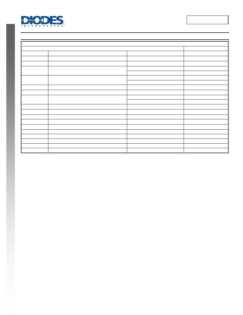
Typical Performance Characteristics
List of Figures
Figure
V
IO
Input Offset Voltage
vs. free air temperature
1
I
IB
,I
IO
Input Bias Current, Input Offset Current
vs. free air temperature
2
I
DD
Supply Current
vs. supply voltage
3
PSRR
Power Supply Rejection Ratio
vs. frequency
4
vs. free air temperature
5
CMRR
Common Mode Rejection Ratio
vs. frequency
6
vs. free air temperature
7
V
OH
High Level Output Voltage
vs. high level output current
8, 9, 10
V
OL
Low Level Output Voltage
vs. high level output current
11,12,13
SR Slew
Rate
vs. free air temperature
14
vs. supply voltage
15
A
VD,
Φ
Differential Voltage Gain And Phase
vs. frequency
16
Φ
m
Phase Margin
vs. capacitive load
17
—
Gain Bandwidth Product
vs. free air temperature
18
V
n
Equivalent Input Noise Voltage
vs. frequency
19
V
O(PP)
Peak To Peak Output Voltage
vs. frequency
20
—
Voltage Follower Large Signal Pulse Response
—
21, 22
—
Voltage Follower Small Signal Pulse Response
—
23
—
Inverting Large Signal Response
—
24, 25
—
Inverting Small Signal Response
—
26
— Crosstalk
vs.
frequency
27