Application information – Diodes TLV27x User Manual
Page 13
TLV271/ TLV272
Document number: DS35394 Rev. 4 - 2
13 of 17
December 2013
© Diodes Incorporated
NEW PROD
UC
T
TLV271/TLV272
Application Information
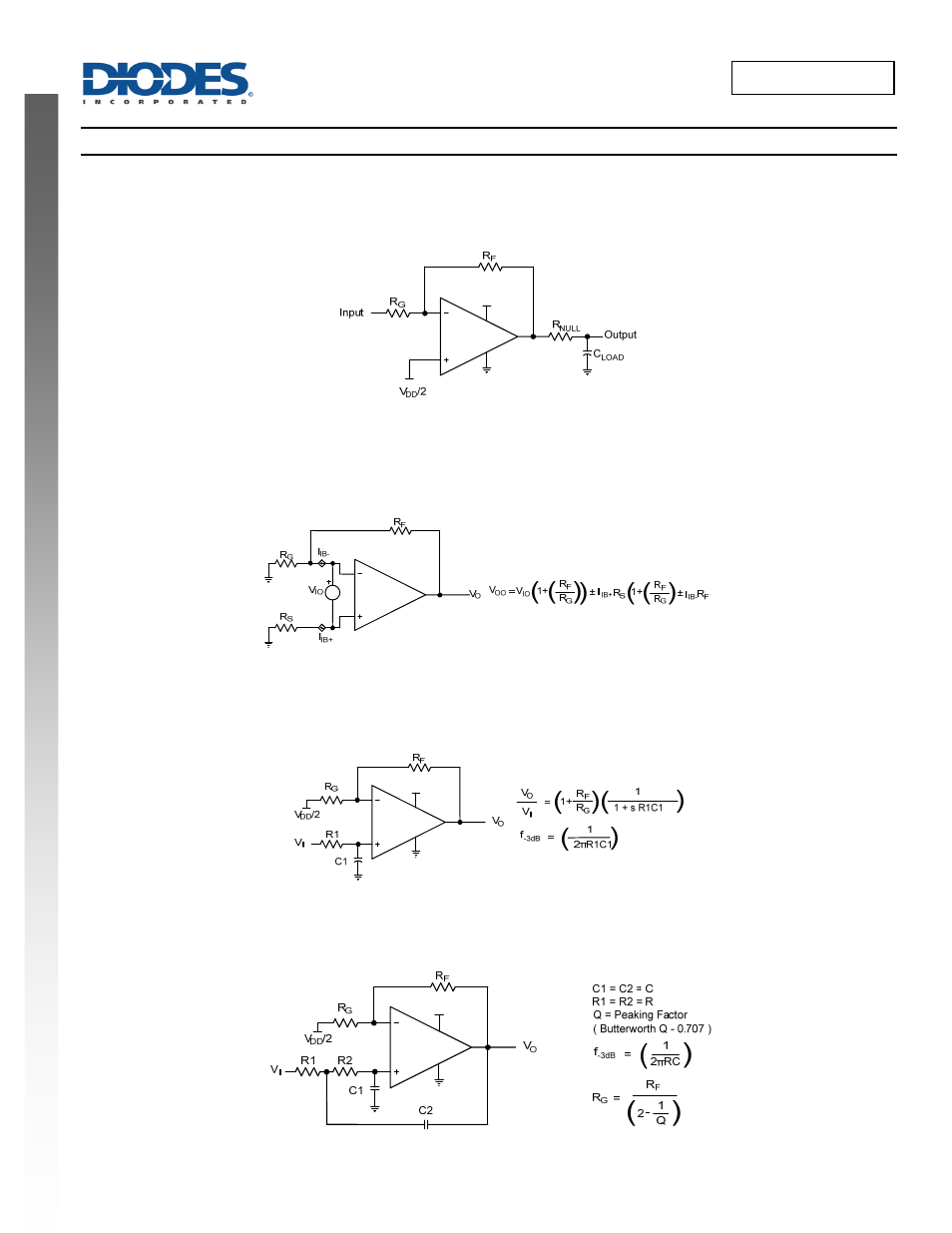
Driving a Capacitive Load
When the amplifier is configured as below, capacitive loading directly on the output can decrease the device’s phase margin leading to high
frequency ringing or oscillations. Therefore, for capacitive loads of greater than 100pF, it is recommended that a resistor be placed in series (R
NULL
)
with the output of the amplifier, as shown in Figure 25. A minimum value of 20Ω should work well for most applications.
Figure 28 Driving a Capacitive Load
Offset Voltage
The output offset voltage, (V
OO
) is the sum of the input offset voltage (V
IO
) and both input bias currents (I
IB
) times the corresponding gains. The
following schematic and formula can be used to calculate the output offset voltage:
Figure 29 Output Offset Voltage Model
Other Configurations
When receiving low-level signals, limiting the bandwidth of the incoming signals into the system is often required. The simplest way to accomplish
this is to place an RC filter at the non-inverting terminal of the amplifier (see Figure 30).
Figure 30. Single Pole Low Pass Filter
If even more attenuation is needed, a multiple pole filter is required. The Sallen-Key filter can be used for this task. For best results, the amplifier
should have a bandwidth that is 8 to 10 times the filter frequency bandwidth. Failure to do this can result in phase shift of the amplifier.
Figure 31. 2-Pole Low-Pass Sallen-Key Filter