Application information, Minimum copper area characteristics – Diodes ZXMS6001N3 User Manual
Page 6
ZXMS6001N3
© Zetex Semiconductors plc 2008
Application information
The current-limit protection circuitry is designed to de-activate at low Vds to prevent the load
current from being unnecessarily restricted during normal operation. The design max DC
operating current is therefore determined by the thermal capability of the package/board
combination, rather than by the protection circuitry (see graph page 8 'typical output
characteristic'). This does not compromise the products ability to self protect at low V
DS
.
The overtemperature protection circuit trips at a minimum of 150°C. So the available package
dissipation reduces as the maximum required ambient temperature increases. This leads to the
following maximum recommended continuous operating currents.
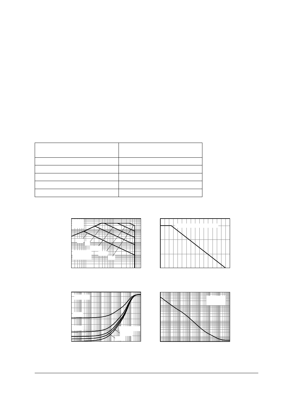
Minimum copper area characteristics
For minimum copper condition as described in note (c)
Max Ambient Temperature T
A
Maximum continuous current
V
IN
=5V
25°C at Vin=5V
720
70°C at Vin=5V
575
85°C at Vin=5V
520
125°C at Vin=5V
320
1
10
100
1m
10m
100m
1
1ms
Single Pulse
T
amb
=25°C
R
DS(on)
Limited
10ms
100ms
1s
Safe Operating Area
I
D
D
rain C
urre
nt
(
A
)
V
DS
Drain-Source Voltage (V)
DC
0
20
40
60
80
100
120
140
160
0.0
0.2
0.4
0.6
see note (c) - Minimum Copper
Derating Curve
Temperature (°C)
Max
P
ow
er D
iss
ip
at
ion (W
)
100µ
1m
10m 100m
1
10
100
1k
0
50
100
150
200
T
amb
=25°C
Transient Thermal Impedance
D=0.5
D=0.2
D=0.1
Single Pulse
D=0.05
Thermal Re
s
is
tan
ce
(°
C/
W
)
Pulse Width (s)
100µ
1m
10m 100m
1
10
100
1k
1
10
100
Single Pulse
T
amb
=25°C
Pulse Power Dissipation
Pulse Width (s)
Maximu
m
P
o
w
er (
W
)