Absolute maximum ratings, Thermal resistance, Absolute maximum ratings thermal resistance – Diodes ZXMS6001N3 User Manual
Page 3
ZXMS6001N3
© Zetex Semiconductors plc 2008
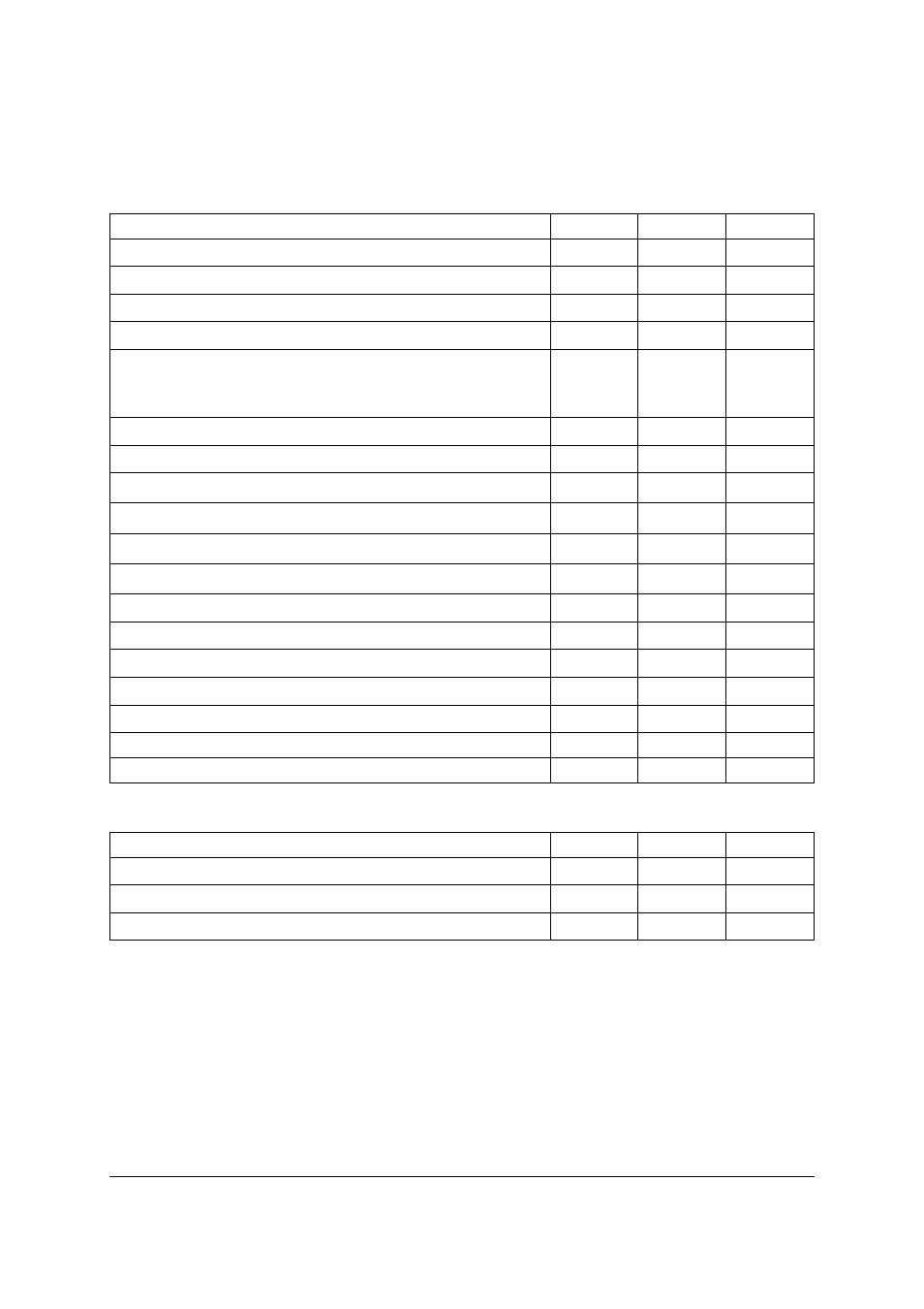
Absolute maximum ratings
Thermal resistance
NOTES:
(a) For a device surface mounted on 25mm x 25mm x 1.6mm FR4 board with a high coverage of single sided 2oz weight
copper. Allocation of 6cm
2
copper 33% to source tab and 66% to drain pin with source tab and drain pin electrically
isolated.
(b) For a device surface mounted on FR4 board as (a) and measured at t<=10s.
(c) For a device surface mounted on FR4 board with the minimum copper required for electrical connections.
Parameter
Symbol
Limit
Unit
Continuous Drain-Source Voltage
V
DS
60
V
Drain-Source Voltage for short circuit protection V
IN
= 5V
V
DS(SC)
36
V
Continuous Input Voltage
V
IN
-0.2 ... +10
V
Peak Input Voltage
V
IN
-0.2 ... +20
V
Continuous Input Current
-0.2V=V
IN
=10V
V
IN
<-0.2V or V
IN
>10V
I
IN
No limit
|
I
IN
|
≤
2
mA
Operating Temperature Range
T
j
,
-40 to +150
°C
Storage Temperature Range
T
stg
-55 to +150
°C
Power Dissipation at T
A
=25
°C
P
D
1.5
W
Power Dissipation at T
A
=25
°C
(c)
P
D
0.6
W
Continuous Drain Current @ V
IN
=5V; T
A
=25
°C
(a)
I
D
1.1
A
Continuous Drain Current @ V
IN
=5V; T
A
=25
°C
(c)
I
D
0.7
A
Continuous Source Current (Body Diode)
(a)
I
S
2.0
A
Pulsed Source Current (Body Diode)
(b)
I
S
3.3
A
Unclamped single pulse inductive energy
E
AS
550
mJ
Load dump protection
V
LoadDump
80
V
Electrostatic Discharge (Human Body Model)
V
ESD
4000
V
DIN humidity category, DIN 40 040
E
IEC climatic category, DIN IEC 68-1
40/150/56
Parameter
Symbol
Value
Unit
Junction to ambient
(a)
R
⍜JA
83
°C/W
Junction to ambient
(b)
R
⍜JA
45
°C/W
Junction to ambient
(c)
R
⍜JA
208
°C/W