Application information – Diodes ZXGD3105N8 User Manual
Page 9
ZXGD3105N8
Document Number DS35101
Rev. 3 - 2
9 of 14
March 2013
© Diodes Incorporated
A Product Line of
Diodes Incorporated
ZXGD3105N8
Application Information
(cont.)
Functional Descriptions for Resonant Converter
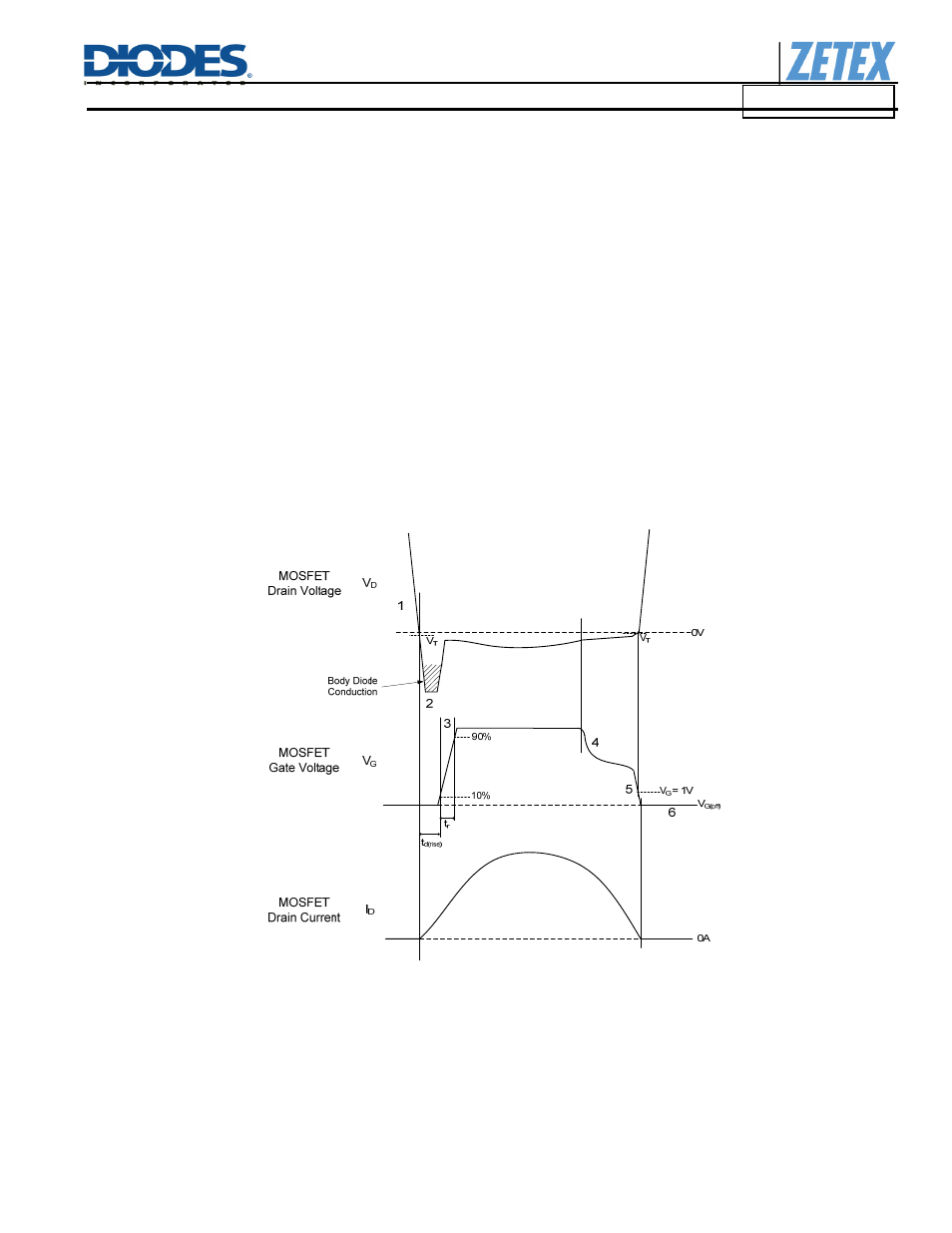
The operation of the ZXGD3105 in resonant converter is described with reference to Figure 4.
1. The detector stage monitors the MOSFET Drain-GND voltage.
2. When, due to transformer action, the MOSFET body diode is forced to conduct there is a negative voltage on the Drain pin due to the
body diode forward voltage.
3. As the negative Drain voltage crosses the Threshold voltage V
T
, the detector stage outputs a positive voltage with respect to ground
after the turn-on delay time t
d(rise)
. This voltage is then fed to the MOSFET driver stage and current is sourced out of the GATE pin.
4. The controller goes into Proportional Gate Drive control. The GATE voltage now varies according to the MOSFET’s Drain-GND
voltage. During this phase, the relationship of V
G
vs. V
D
is shown by the transfer characteristic curve in page xx of this datasheet. As
the Drain current decays linearly, the Gate voltage reduces so the MOSFET can be turned off rapidly at zero current crossing.
Proportional Gate Drive also ensures that gate voltage is supplied to the MOSFET gate until the Drain current is virtually zero. This
eliminates any parasitic diode conduction after the MOSFET switches off.
5. The GATE voltage falls to 1V when the Drain-GND voltage reaches V
T
. The MOSFET is turned off precisely when the sinusoidal
current goes to zero, with little or no reverse current. Threshold voltage V
T
is defined as the Drain voltage V
D
level at which Gate
voltage V
G
is 1V (refer to electrical characteristic section in page 4).
6. At zero Drain current, the GATE voltage is pulled low to V
G(off)
to ensure that the MOSFET is off.
Figure 4 Timing diagram of synchronous rectification in the resonant converter