Application information – Diodes ZXGD3105N8 User Manual
Page 11
ZXGD3105N8
Document Number DS35101
Rev. 3 - 2
11 of 14
March 2013
© Diodes Incorporated
A Product Line of
Diodes Incorporated
ZXGD3105N8
Application Information
(cont.)
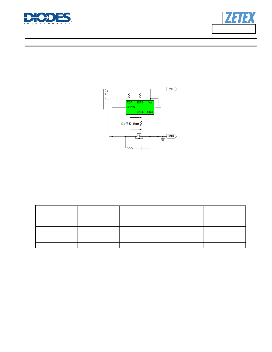
Gate Driver
The controller is provided with single channel high current gate drive output, capable of driving one or more N-channel power MOSFETs. The
controller can operate from Vcc of 4.5V to drive both standard MOSFETs and logic level MOSFETs.
The Gate pins should be as close to the MOSFET’s gate as possible. A resistor in series with GATE pin helps to control the rise time and
decrease switching losses due to gate voltage oscillation. A diode in parallel to the resistor is typically used to maintain fast discharge of the
MOSFET’s gate.
Figure 6 Typical connection of the ZXGD3105 to the synchronous MOSFET
Quiescent Current Consumption
The quiescent current consumption of the controller is the sum of I
REF
and I
BIAS
. For an application that requires ultra-low standby power
consumption, I
REF
and I
BIAS
can be further reduced by increasing the value of resistor R
REF
and R
BIAS
.
Bias Current, I
BIAS
(mA)
Ref Current, I
REF
(mA)
Bias Resistor, R
BIAS
(kΩ)
Ref Resistor, R
REF
(kΩ)
Quiescent Current, I
Q
(mA)
0.25 0.61 39.2 15.4 0.86
0.35 0.81 28.0 11.5 1.16
0.46 0.99 21.5 9.3 1.45
0.50 1.00 19.6 8.9 1.50
0.55 1.13 17.8 8.1 1.68
0.80 1.66 12.1 5.6 2.46
Table 2 Quiescent current consumption for different resistor values at V
CC
= 10V
I
REF
also controls the gate driver peak sink current whilst I
BIAS
controls the peak source current. At the default current value of I
REF
and I
BIAS
of
1.02mA and 0.54mA, the gate driver is able to provide 2A source and 6A sink current. The gate current decreases if I
REF
and I
BIAS
are reduced.
Care must be taken in reducing the controller quiescent current so that sufficient drive current is still delivered to the MOSFET particularly for high
switching frequency application.