Application information – Diodes ZXGD3105N8 User Manual
Page 8
ZXGD3105N8
Document Number DS35101
Rev. 3 - 2
8 of 14
March 2013
© Diodes Incorporated
A Product Line of
Diodes Incorporated
ZXGD3105N8
Application Information
(cont.)
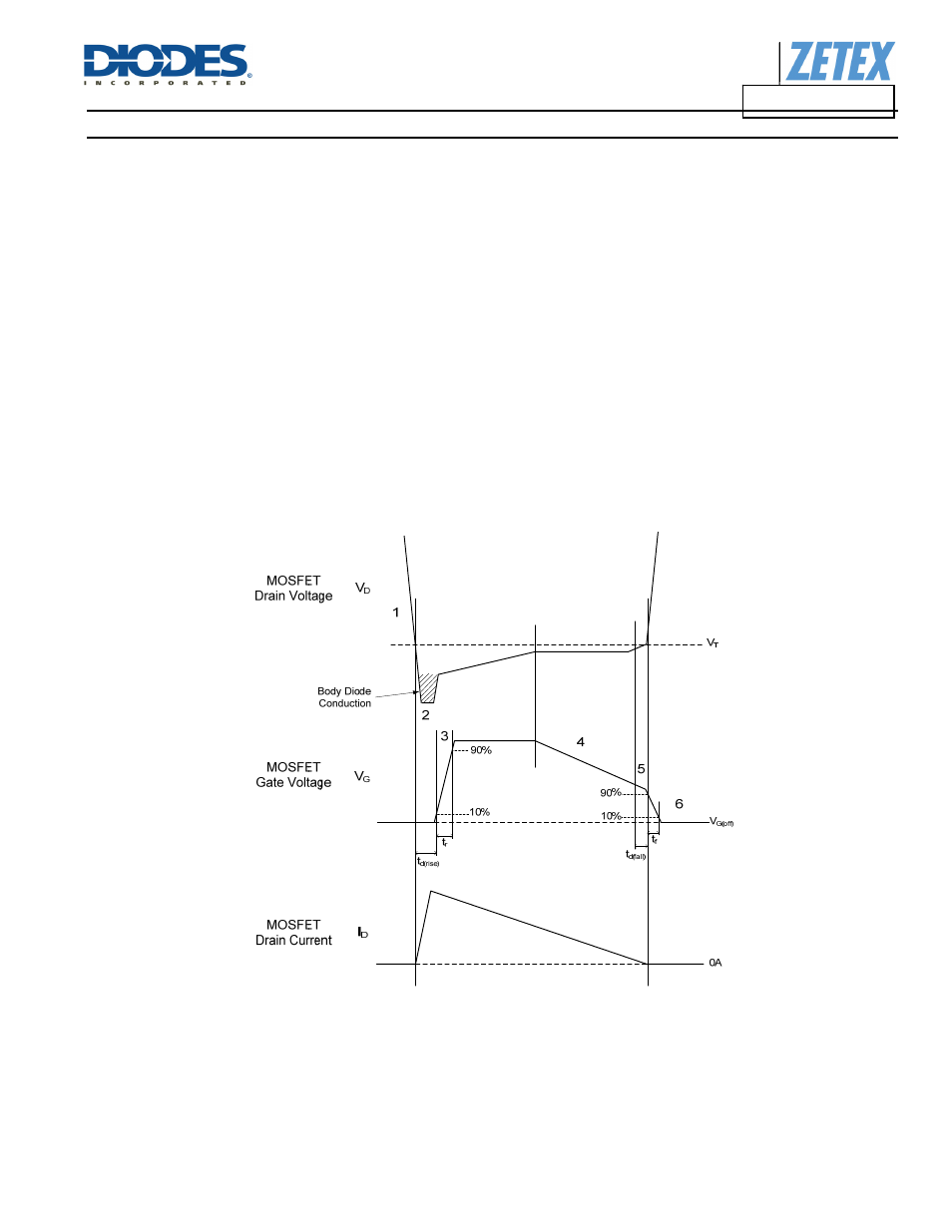
Functional Descriptions for Flyback Converter
The operation of the device is described step-by-step with reference to the timing diagram in Figure 3.
1. The detector stage monitors the MOSFET Drain-Source voltage.
2. When, due to transformer action, the MOSFET body diode is forced to conduct there is a negative voltage on the Drain pin due to the
body diode forward voltage.
3. As the negative Drain voltage crosses the turn-off Threshold voltage V
T
, the detector stage outputs a positive voltage with respect to
ground after the turn-on delay time t
d(fall)
. This voltage is then fed to the MOSFET driver stage and current is sourced out of the
GATE pin.
4. The controller goes into proportional gate drive control — the GATE output voltage is proportional to the MOSFET on-resistance-
induced Drain-Source voltage. Proportional gate drive ensures that MOSFET conducts during the majority of the conduction cycle to
minimize power loss in the body diode.
5. As the Drain current decays linearly toward zero, proportional gate drive control reduces the Gate voltage so the MOSFET can be
turned off rapidly at zero current crossing. The GATE voltage falls to 1V when the Drain-Source voltage crosses the detection
threshold voltage to minimize reverse current flow.
6. At zero Drain current, the controller GATE output voltage is pulled low to V
G(off)
to ensure that the MOSFET is off.
Figure 3 Timing diagram for a critical conduction mode Flyback converter