Thermal derating curve, Electrical characteristics, Derating curve – Diodes ZXGD3105N8 User Manual
Page 4
ZXGD3105N8
Document Number DS35101
Rev. 3 - 2
4 of 14
March 2013
© Diodes Incorporated
A Product Line of
Diodes Incorporated
ZXGD3105N8
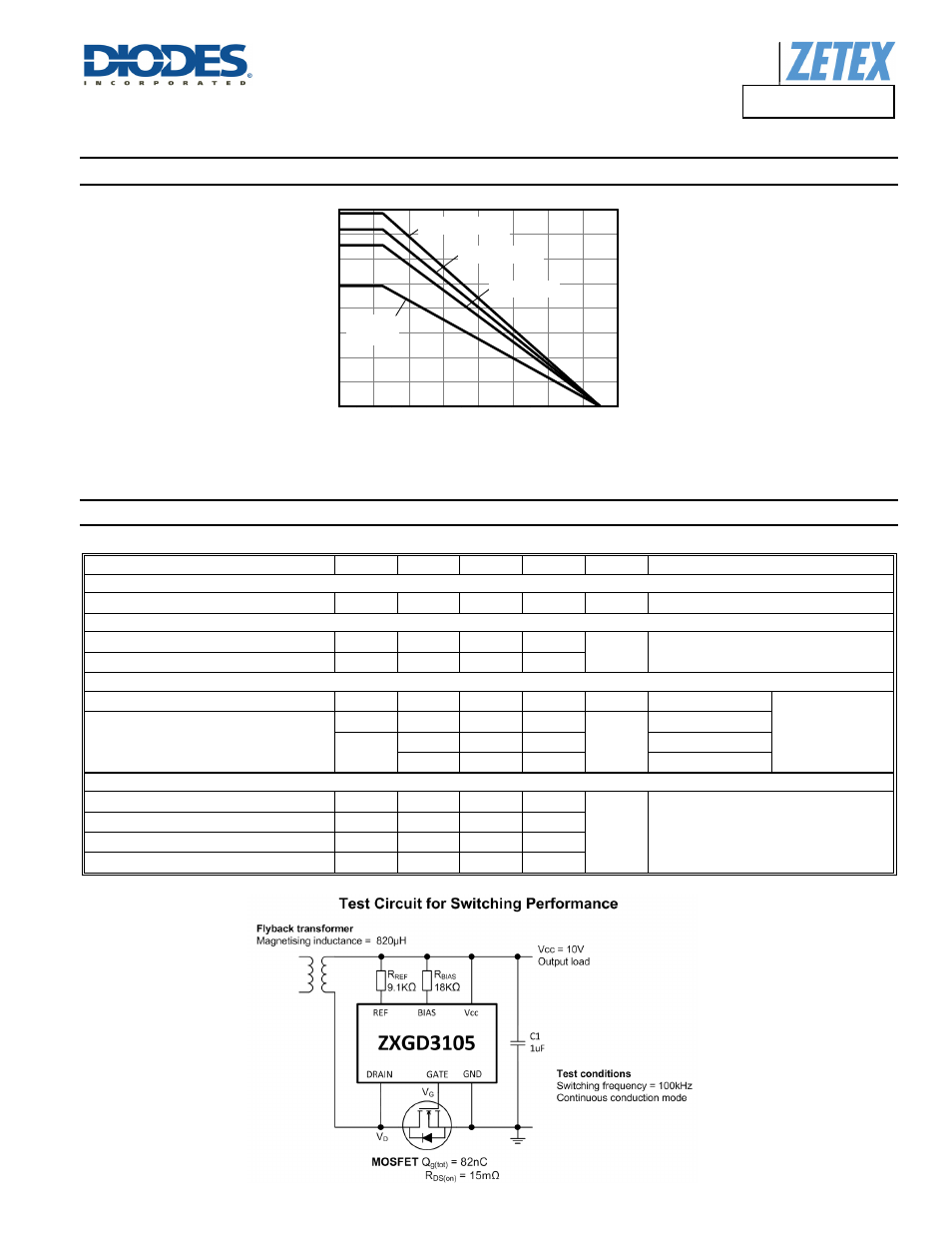
Thermal Derating Curve
Electrical Characteristics
(@T
A
= +25°C, unless otherwise specified.)
V
CC
= 10V; R
BIAS
= 18kΩ (I
BIAS
= 0.54mA); R
REF
= 9.1kΩ (I
REF
= 1.02mA)
Characteristic Symbol
Min
Typ
Max
Unit Test
Condition
Input Supply
Quiescent current
I
Q
— 1.56 — mA
V
DRAIN
≥ 0mV
Gate Driver
Gate peak source current
I
SOURCE
— 1.2 —
A
Capacitive load: C
L
= 10nF
Gate peak sink current
I
SINK
— 5 —
Detector under DC condition
Turn-off Threshold Voltage
V
T
-20 -10 0 mV
V
G
= 1V
Capacitive load only
Gate output voltage
V
G(off)
— 0.2 0.6
V
V
DRAIN
≥ 1V
V
G
5.0 7.8 —
V
DRAIN
= -50mV
8.0 9.4 —
V
DRAIN
= -100mV
Switching Performance
Turn-on propagation delay
t
d(rise)
— 118 —
ns
Capacitive load: C
L
= 10nF
Rise and fall measured 10% to 90%
Gate rise time
t
r
— 77 —
Turn-off propagation delay
t
d(fall)
— 14 —
Gate fall time
t
f
— 26 —
0
20
40
60
80
100 120 140 160
0.0
0.1
0.2
0.3
0.4
0.5
0.6
0.7
0.8
15mm x 15mm
5mm x 5mm
Minimum
Layout
Derating Curve
Junction Temperature (°C)
M
ax P
o
wer
Di
ssi
pat
io
n (W)
10mm x 10mm