Functional block diagram – Diodes ZXGD3105N8 User Manual
Page 2
ZXGD3105N8
Document Number DS35101
Rev. 3 - 2
2 of 14
March 2013
© Diodes Incorporated
A Product Line of
Diodes Incorporated
ZXGD3105N8
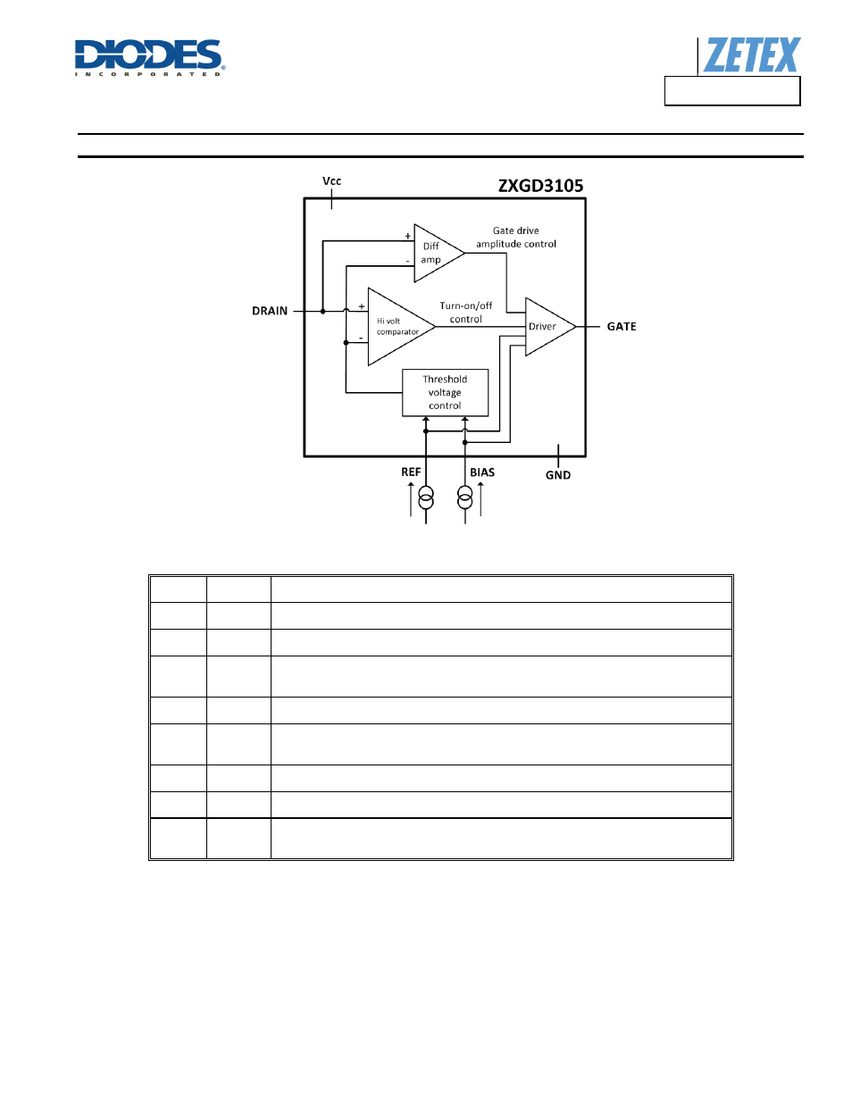
Functional Block Diagram
Pin
Number
Pin
Name
Description
1
V
CC
Power supply
This supply pin should be closely decoupled to ground with a ceramic capacitor.
2 DNC
Do not connect
Leave pin floating.
3 BIAS
Bias
Connect this pin to V
CC
via R
BIAS
resistor. Select R
BIAS
to source 0.54mA into this pin.
Refer to Table 1 and 2, in Application Information section.
4 DRAIN
Drain sense
Connect directly to the synchronous MOSFET drain terminal.
5 REF
Reference
Connect this pin to V
CC
via R
REF
resistor. Select R
REF
to source 1.02mA into this pin.
Refer to Table 1 and 2, in Application Information section.
6 DNC
Do not connect
Leave pin floating.
7 GND
Ground
Connect this pin to the synchronous MOSFET source terminal and ground reference point.
8 GATE
Gate drive
This pin sinks and sources the I
SINK
and I
SOURCE
current to the synchronous MOSFET
gate.