Tvs diode arrays, Lightning surge protection - spl v2.8 series, F amily of products) – Littelfuse SPLV2.8 Series User Manual
Page 2
©2012 Littelfuse, Inc.
Specifications are subject to change without notice.
Please refer to
www.littelfuse.com/SPA
for current information.
140
TVS Diode Arrays
(SPA
™
F
Revision: March 20, 2012
SPLV2.8 Series
Lightning Surge Protection - SPL
Absolute Maximum Ratings
Parameter
Rating
Units
Peak Pulse Power (t
P
=8/20μs)
600
W
Peak Pulse Current (t
P
=8/20μs)
40
A
Operating Temperature
-40 to 85
ºC
Storage Temperature
-60 to 150
ºC
Electrical Characteristics (T
OP
= 25°C)
Parameter
Symbol
Test Conditions
Min
Typ
Max
Units
Reverse Standoff Voltage
V
RWM
I
R
≤1μA
2.8
V
Reverse Breakdown Voltage
V
BR
I
T
=2μA
3.0
V
Snap Back Voltage
V
SB
I
T
=50mA
2.8
V
Reverse Leakage Current
I
LEAK
V
R
=2.8V (Pin 2 or 3 to 1)
1
μA
Clamping Voltage
1
V
C
I
PP
=5A, t
P
=8/20μs (Pin 3 to 1)
5.7
7.0
V
Clamping Voltage
1
I
PP
=24A, t
P
=8/20μs (Pin 3 to 1)
8.3
12.5
V
Clamping Voltage
1
I
PP
=5A, t
P
=8/20μs (Pin 2 to 1)
7.0
8.5
V
Clamping Voltage
1
I
PP
=24A, t
P
=8/20μs (Pin 2 to 1)
13.9
15.0
V
Dynamic Resistance
R
DYN
(V
C2
- V
C1
) / (I
PP2
- I
PP1
) (Pin 2 to 1)
0.4
Ω
ESD Withstand Voltage
1
V
ESD
IEC61000-4-2 (Contact)
±30
kV
IEC61000-4-2 (Air)
±30
kV
Diode Capacitance
1
C
D
V
R
=0V, f=1MHz (Pin 2 to 1)
2.0
2.5
pF
CAUTION: Stresses above those listed in “Absolute Maximum Ratings” may cause
permanent damage to the device. This is a stress only rating and operation of the device
at these or any other conditions above those indicated in the operational sections of this
specification is not implied.
Note:
1
Parameter is guaranteed by design and/or device characterization.
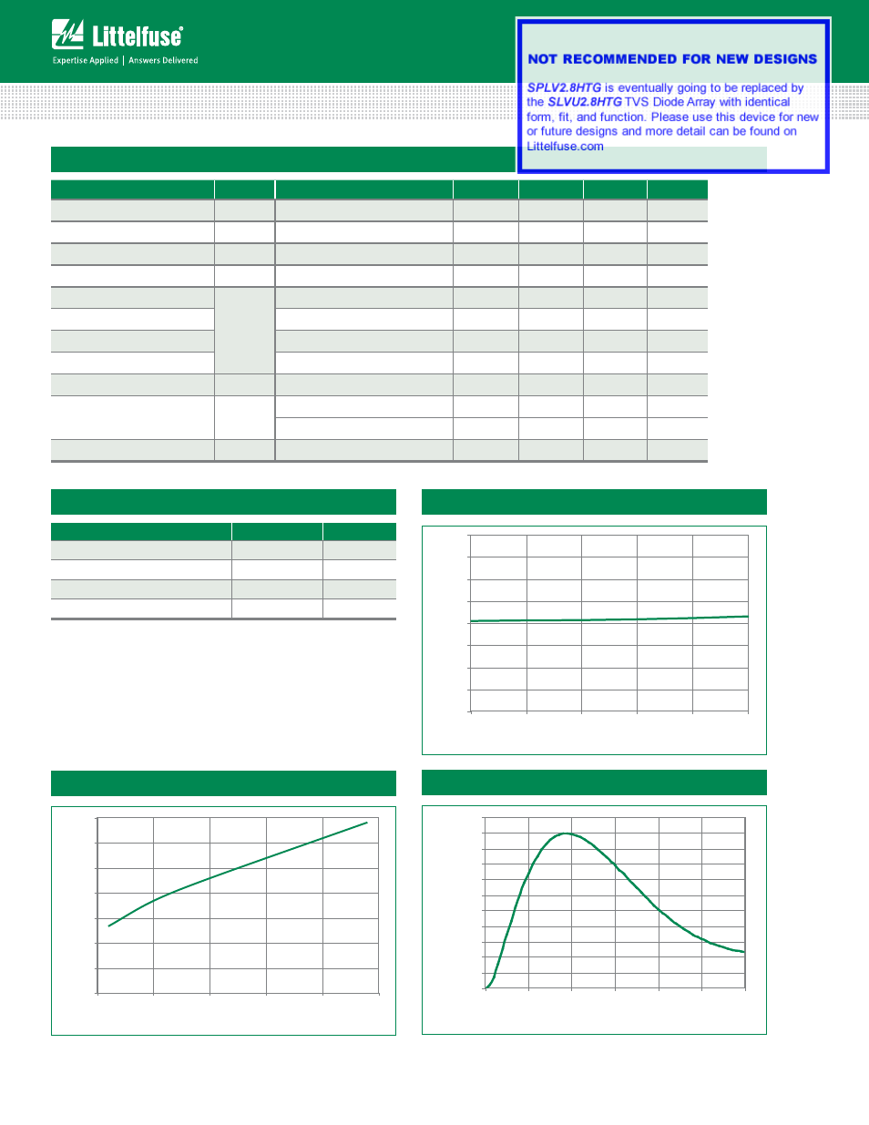
Figure 2: Clamping Voltage vs. I
PP
Figure 1: Capacitance vs. Reverse Voltage
Figure 3: Pulse Waveform
0.0
0.5
1.0
1.5
2.0
2.5
3.0
3.5
4.0
0.0
0.5
1.0
1.5
2.0
2.5
DC Bias (V)
Capacitance (pF)
0%
10%
20%
30%
40%
50%
60%
70%
80%
90%
100%
110%
0.0
5.0
10.0
15.0
20.0
25.0
30.0
Time (μs)
P
e
rc
ent of I
PP
0
2
4
6
8
10
12
14
0
5
10
15
20
25
Peak Pulse Current-I
PP
(A)
Clamping Voltage-V
C
(V)