Tvs diode arrays, Low capacitance esd protection - sp3012 series, Diodes) – Littelfuse SP3012 Series User Manual
Page 5: Sp30 1 2, User feeding direction pin 1 location
5
©2013 Littelfuse, Inc.
Specifications are subject to change without notice.
TVS Diode Arrays
(SPA
®
Diodes)
Revision: 09 2, 13
SP3012 Series
SP30
1
2
Low Capacitance ESD Protection - SP3012 Series
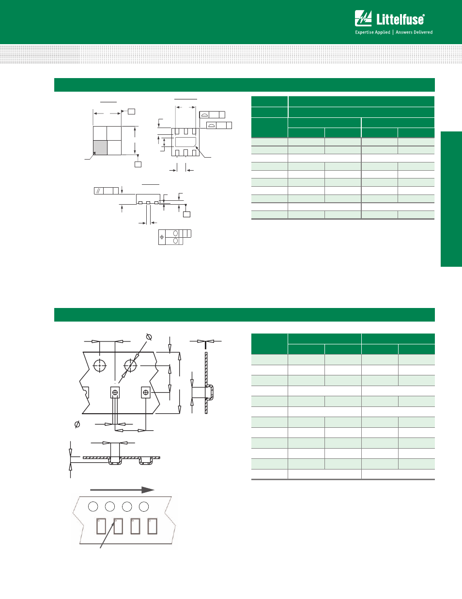
Embossed Carrier Tape & Reel Specification — μDFN-6
K0
A0
B0
P2
D1
P0
t
F
E
W
D
User Feeding Direction
Pin 1 Location
Symbol
Millimetres
Inches
Min
Max
Min
Max
E
1.65
1.85
0.06
0.07
F
3.45
3.55
0.14
0.14
D1
1.00
1.25
0.04
0.05
D
1.50 MIN
0.06 MIN
P0
3.90
4.10
0.15
0.16
10P0
40.0+/- 0.20
1.57+/-0.01
W
7.90
8.30
0.31
0.33
P2
1.95
2.05
0.08
0.08
A0
1.78
1.88
0.07
0.07
B0
1.78
1.88
0.07
0.07
K0
0.84
0.94
0.03
0.04
t
0.25 TYP
0.01 TYP
Package Dimensions — μDFN-6
Package
μDFN-6 (1.6x1.6x0.5mm)
JEDEC
MO-229
Symbol
Millimeters
Inches
Min
Max
Min
Max
A
0.45
0.55
0.018
0.022
A1
0.00
0.05
0.000
0.002
A3
0.152Ref
0.006 Ref
b
0.20
0.30
0.008
0.012
D
1.55
1.65
0.061
0.065
D2
1.05
1.30
0.042
0.052
E
1.50
1.70
0.060
0.067
E2
0.40
0.65
0.016
0.026
e
0.50 BSC
0.020BSC
L
0.164
0.316
0.006
0.012
D
E
B
1
2
3
6
5
4
Top View
Pin 1 Index Area
A
A
1
2
3
5
4
6
L
Pin 1 chamfer
0.10 x 45’
℮
0.05 C
Bottom View
0.05 C
0.05 C
b
A1
A3
C
Seating plane
Side View
0.10
C A
M
B
0.05
C
M
D2
E2