Tvs diode arrays, General purpose esd protection - sp1002 series, Diodes) – Littelfuse SP1002 Series User Manual
Page 3
© 2013 Littelfuse, Inc.
Specifications are subject to change without notice.
Revised: 10/10/13
TVS Diode Arrays
(SPA
®
Diodes)
General Purpose ESD Protection - SP1002 Series
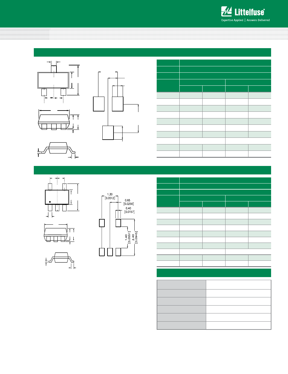
Package Dimensions — SC70-3
B
3
E HE
2
1
e
e
D
A2 A
A1
C
L
1.30
[0.0512]
0.65
[0.0256]
0.70
[0.0276]
1.90
[0.0748]
0.90
[0.0354]
Package
SC70-3
Pins
3
JEDEC
MO-203
Millimeters
Inches
Min
Max
Min
Max
A
0.80
1.10
0.031
0.043
A1
0.00
0.10
0.000
0.004
A2
0.70
1.00
0.028
0.039
B
0.15
0.30
0.006
0.012
c
0.08
0.25
0.003
0.010
D
1.85
2.25
0.073
0.089
E
1.15
1.35
0.045
0.053
e
0.66 BSC
0.026 BSC
HE
2.00
2.40
0.079
0.094
L
0.26
0.46
0.010
0.018
Solder Pad Layout
Package Dimensions — SC70-5
D
A2 A
A1
C
L
E
HE
2
1
3
6
5
not used
4
e
e
B
Package
SC70-5
Pins
5
JEDEC
MO-203
Millimeters
Inches
Min
Max
Min
Max
A
0.80
1.10
0.031
0.043
A1
0.00
0.10
0.000
0.004
A2
0.70
1.00
0.028
0.039
B
0.15
0.30
0.006
0.012
c
0.08
0.25
0.003
0.010
D
1.85
2.25
0.073
0.089
E
1.15
1.35
0.045
0.053
e
0.65 BSC
0.026 BSC
HE
2.00
2.40
0.079
0.094
L
0.26
0.46
0.010
0.018
Solder Pad Layout
Product Characteristics
Lead Plating
Matte Tin
Lead Material
Copper Alloy
Lead Coplanarity
0.0004 inches (0.102mm)
Substitute Material
Silicon
Body Material
Molded Epoxy
Flammability
UL 94 V-0
Notes :
1. All dimensions are in millimeters
2. Dimensions include solder plating.
3. Dimensions are exclusive of mold flash & metal burr.
4. Blo is facing up for mold and facing down for trim/form, i.e. reverse trim/form.
5. Package surface matte finish VDI 11-13.