Tvs diode arrays, General purpose esd protection - sp724 series, Diodes) – Littelfuse SP724 Lead-Free_Green Series User Manual
Page 5: Soldering parameters, Recommended solder pad layout
© 2013 Littelfuse, Inc.
Specifications are subject to change without notice.
Revised: 11/25/13
TVS Diode Arrays
(SPA
®
Diodes)
General Purpose ESD Protection - SP724 Series
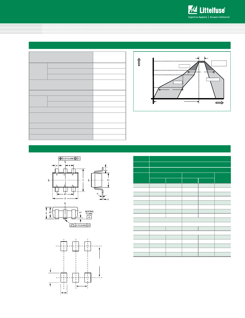
Package Dimensions — Small Outline Transistor Plastic Packages (SOT23-6)
Time
Te
mperatur
e
T
P
T
L
T
S(max)
T
S(min)
25
t
P
t
L
t
S
time to peak temperature
Preheat
Preheat
Ramp-up
Ramp-up
Ramp-down
Ramp-do
Critical Zone
T
L
to T
P
Critical Zone
T
L
to T
P
Reflow Condition
Pb – Free assembly
Pre Heat
- Temperature Min (T
s(min)
)
150°C
- Temperature Max (T
s(max)
)
200°C
- Time (min to max) (t
s
)
60 – 180 secs
Average ramp up rate (Liquidus) Temp
(T
L
) to peak
5°C/second max
T
S(max)
to T
L
- Ramp-up Rate
5°C/second max
Reflow
- Temperature (T
L
) (Liquidus)
217°C
- Temperature (t
L
)
60 – 150 seconds
Peak Temperature (T
P
)
260
+0/-5
°C
Time within 5°C of actual peak
Temperature (t
p
)
20 – 40 seconds
Ramp-down Rate
5°C/second max
Time 25°C to peak Temperature (T
P
)
8 minutes Max.
Do not exceed
260°C
Soldering Parameters
Notes:
1. Dimensioning and tolerances per ANSI 14.5M-1982.
2. Package conforms to EIAJ SC-74 (1992).
3. Dimensions D and E1 are exclusive of mold flash, protrusions, or gate burrs.
4. Footlenth L measured at reference to seating plane.
5. “L” is the length of flat foot surface for soldering to substrate.
6. “N” is the number of terminal positions.
7. Controling dimension: MILLIMETER. Converted inch dimensions are not necessarily
exact.
Package
SOT23-6
Pins
6
JEDEC
MO-178
Millimeters
Inches
Notes
Min
Max
Min
Max
A
0.900
1.450
0.035
0.057
-
A1
0.000
0.150
0.000
0.006
-
A2
0.900
1.300
0.035
0.051
-
b
0.350
0.500
0.0138
0.0196
-
C
0.080
0.220
0.0031
0.009
-
D
2.800
3.000
0.11
0.118
3
E
2.600
3.000
0.102
0.118
-
E1
1.500
1.750
0.06
0.069
3
e
0.95 Ref
0.0374 ref
-
e1
1.9 Ref
0.0748 Ref
-
L
0.100
0.600
0.004
0.023
4,5
N
6
6
6
a
0º
10º
0º
10º
-
M
2.590
0.102
-
O
0.690
.027 TYP
-
P
0.990
.039 TYP
-
R
0.950
0.038
-
O
P
R
M
Recommended Solder Pad Layout