Tvs diode arrays, General purpose esd protection - sp721 series, Diodes) – Littelfuse SP721 Lead-Free_Green Series User Manual
Page 4
© 2013 Littelfuse, Inc.
Specifications are subject to change without notice.
Revised: 04/24/13
TVS Diode Arrays
(SPA
®
Diodes)
General Purpose ESD Protection - SP721 Series
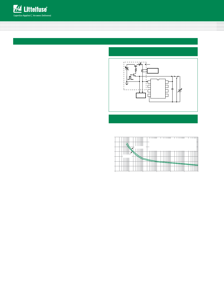
Peak Transient Current Capability of the SP721
The peak transient current capability rises sharply as the
width of the current pulse narrows. Destructive testing
was done to fully evaluate the SP721’s ability to withstand
a wide range of peak current pulses vs time. The circuit
used to generate current pulses is shown in Figure 4.
The test circuit of Figure 4 is shown with a positive pulse
input. For a negative pulse input, the (-) current pulse input
goes to an SP721 ‘IN’ input pin and the (+) current pulse
input goes to the SP721 V- pin. The V+ to V- supply of the
SP721 must be allowed to float. (i.e., It is not tied to the
ground reference of the current pulse generator.) Figure
5 shows the point of overstress as defined by increased
leakage in excess of the data sheet published limits.
The maximum peak input current capability is dependent
on the ambient temperature, improving as the temperature
is reduced. Peak current curves are shown for ambient
temperatures of 25ºC and 105ºC and a 15V power supply
condition. The safe operating range of the transient peak
current should be limited to no more than 75% of the
measured overstress level for any given pulse width as
shown in the curves of Figure 5.
Note that adjacent input pins of the SP721 may be
paralleled to improve current (and ESD) capability. The
sustained peak current capability is increased to nearly
twice that of a single pin.
+
-
VOLTAGE
PROBE
+
-
R
1
~ 10 TYPICAL
V
X
V
X
ADJ. 10V/A TYPICAL
R
1
(-)
(+)
C1 ~ 100 µF
C1
VARIABLE TIME DURATION
CURRENT PULSE GENERA TOR
1
2
3
4
8
7
6
5
V+
IN
IN
IN
IN
IN
IN
V-
SP721
CURRENT
SENSE
FIGURE 5. TYPICAL SP721 PEAK CURRENT TEST CIRCUIT
WITH A VARIABLE PULSE WIDTH INPUT
0.001
0.01
0.1
1
10
7
6
5
4
3
2
1
0
100
1000
CAUTION: SAFE OPERATING CONDITIONS LIMIT
THE MAXIMUM PEAK CURRENT FOR A GIVEN
PULSE WIDTH TO BE NO GREATER THAN 75%
OF THE VALUES SHOWN ON EACH CURVE.
V+ TO V-SUPPLY = 15V
T
A
= 25°C
T
A
= 105°C
PULSE WIDTH TIME (ms)
PEAK CURRENT (A)
Showing the Measured Point of Overstress in Amperes vs
pulse width time in milliseconds
Figure 5: SP721 Typical Single Peak Current Pulse
Capability
Figure 4: Typical SP721 Peak Current Test Circuit
with a Variable Pulse Width Input