Tvs diode arrays, Lightning surge protection - sp4040 series, F amily of products) – Littelfuse SP4040 Series User Manual
Page 2: Sp4040
©2012 Littelfuse, Inc.
Specifications are subject to change without notice.
Please refer to
www.littelfuse.com/SPA
for current information.
152
TVS Diode Arrays
(SPA
™
F
Revision: March 20, 2012
SP4040 Series
SP4040
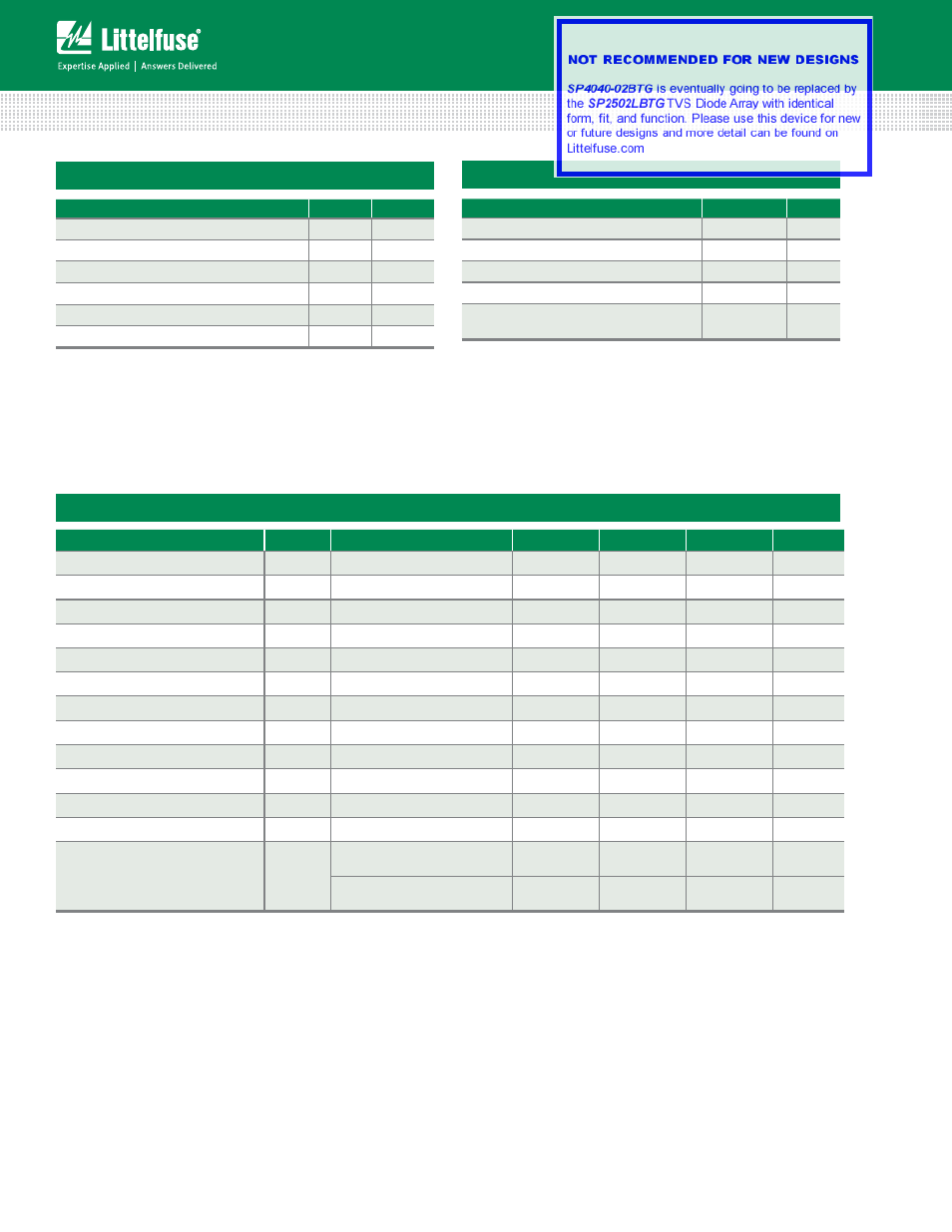
Absolute Maximum Ratings
Parameter
Rating
Units
Peak Pulse Current (8/20μs)
75
A
Peak Pulse Power (8/20μs)
2100
W
IEC 61000-4-2, Direct Discharge, (Level 4)
30
kV
IEC 61000-4-2, Air Discharge, (Level 4)
30
kV
Telcordia GR 1089 (Intra-Building) (2/10μs)
100
A
ITU K.20 (5/310μs)
20
A
Electrical Characteristics (T
OP
= 25°C)
Thermal Information
Parameter
Rating
Units
SOIC Package
170
°C/W
Operating Temperature Range
-55 to 125
°C
Storage Temperature Range
-65 to 150
°C
Maximum Junction Temperature
150
°C
Maximum Lead Temperature (Soldering
20-40s) (SOIC - Lead Tips Only)
260
°C
Parameter
Symbol
Test Conditions
Min
Typ
Max
Units
Reverse Stand-Off Voltage
V
RWM
I
T
≤1μA
-
-
3.3
V
Reverse Breakdown Voltage
V
BR
I
T
= 2μA
3.3
-
-
V
Snap Back Voltage
V
SB
I
T
= 50mA
3.3
-
-
V
Reverse Leakage Current
I
R
V
RWM
= 3.3V
-
-
1
μA
Clamping Voltage, Line-Ground
1
V
C
I
PP
= 40A, t
p
=8/20 μs
-
-
14
V
Clamping Voltage, Line-Ground
1
V
C
I
PP
= 75A, t
p
=8/20 μs
-
-
20
V
Clamping Voltage, Line-Ground
1
V
C
I
PP
= 100A, t
p
=2/10 μs
20
V
Dynamic Resistance, Line-Ground
1
R
DYN
( V
C2
-V
C1
)/(I
PP2
-I
PP1
)
-
0.2
-
Clamping Voltage, Line-Line
1
V
C
I
PP
= 40A, t
p
=8/20 μs
-
-
20
V
Clamping Voltage, Line-Line
1
V
C
I
PP
= 75A, t
p
=8/20 μs
-
-
30
V
Clamping Voltage, Line-Line
1
V
C
I
PP
= 100A, t
p
=2/10 μs
30
V
Dynamic Resistance, Line-Line
1
R
DYN
( V
C2
-V
C1
)/(I
PP2
-I
PP1
)
-
0.3
-
Junction Capacitance
1
C
j
Line to Ground
V
R
=0V, f= 1MHz
-
5
8
pF
Line to Line, V
R
=0V, f= 1MHz
-
2.5
5
pF
CAUTION: Stresses above those listed in “Absolute Maximum Ratings” may cause
permanent damage to the device. This is a stress only rating and operation of the device
at these or any other conditions above those indicated in the operational sections of this
specification is not implied.
1
Parameter is guaranteed by design and/or device characterization.