Tvs diode arrays, General purpose esd protection - sp1001 series, Diodes) – Littelfuse SP1001 Series User Manual
Page 2
© 2013 Littelfuse, Inc.
Specifications are subject to change without notice.
Revised: 10/10/13
TVS Diode Arrays
(SPA
®
Diodes)
General Purpose ESD Protection - SP1001 Series
Absolute Maximum Ratings
Symbol
Parameter
Value
Units
I
PP
Peak Current (t
p
=8/20μs)
2
A
T
OP
Operating Temperature
–40 to 125
°C
T
STOR
Storage Temperature
–55 to 150
°C
CAUTION: Stresses above those listed in “Absolute Maximum Ratings” may cause
permanent damage to the device. This is a stress only rating and operation of the device
at these or any other conditions above those indicated in the operational sections of this
specification is not implied.
Electrical Characteristics (T
OP
= 25°C)
Parameter
Symbol
Test Conditions
Min
Typ
Max
Units
Forward Voltage Drop
V
F
I
F
=10mA
0.7
0.9
1.2
V
Reverse Voltage Drop
V
R
I
R
=1mA
6.0
8.5
V
Reverse Standoff Voltage
V
RWM
I
R
≤1µA
5.5
V
Reverse Leakage Current
I
LEAK
V
R
=5V
0.5
µA
Clamp Voltage
1
V
C
I
PP
=1A, t
p
=8/20µs, Fwd
8.0
11.0
V
I
PP
=2A, t
p
=8/20µs, Fwd
9.7
13.0
V
Dynamic Resistance
R
DYN
(V
C2
- V
C1
) / (I
PP2
- I
PP1
)
1.7
Ω
ESD Withstand Voltage
1,2
V
ESD
IEC61000-4-2 (Contact)
±15
kV
IEC61000-4-2 (Air)
±30
kV
Diode Capacitance
1
C
D
Reverse Bias=0V
12
pF
Reverse Bias=2.5V
8
pF
Reverse Bias=5V
7
pF
Notes:
1
Parameter is guaranteed by device characterization
2
A minimum of 1,000 ESD pulses are applied at 1s intervals between the anode and common cathode of each diode
Thermal Information
Parameter
Rating
Units
Storage Temperature Range
–55 to 150
°C
Maximum Junction Temperature
150
°C
Maximum Lead Temperature (Soldering
20s-40s)
260
°C
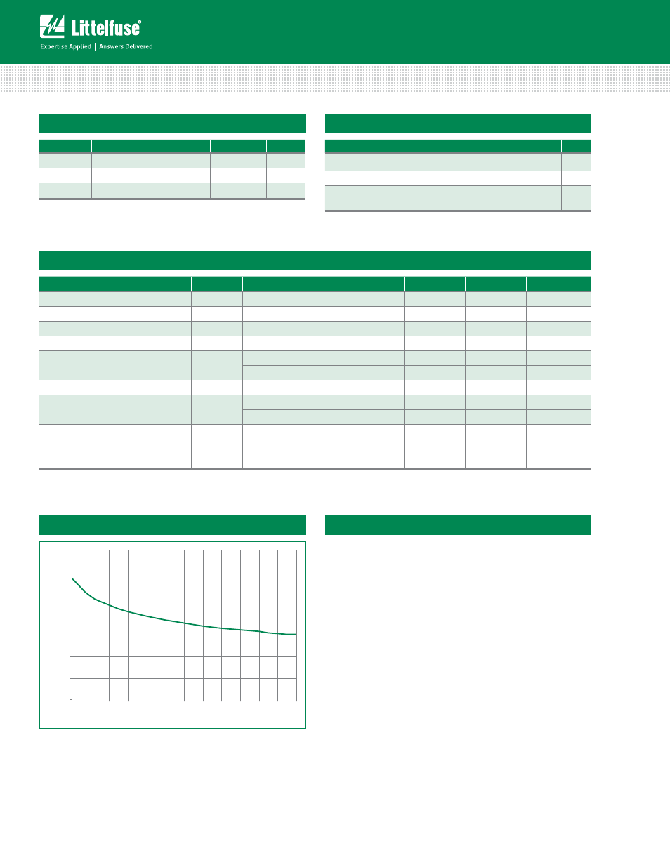
Capacitance vs. Reverse Bias
0
2
4
6
8
10
12
14
DC Bias (V)
Capacitance (pF)
0
0.5
1
1.5
2
2.5
3
3.5
4
4.5
5
5.5
6
Design Consideration
Because of the fast rise-time of the ESD transient,
placement of ESD devices is a key design consideration.
To achieve optimal ESD suppression, the devices should be
placed on the circuit board as close to the source of the ESD
transient as possible. Install the ESD suppressors directly
behind the connector so that they are the first board-level
circuit component encountered by the ESD transient. They
are connected from signal/data line to ground.