Tvs diode arrays, Low capacitance esd protection - sp3002 series, Diodes) – Littelfuse SP3002 Series User Manual
Page 4
© 2013 Littelfuse, Inc.
Specifications are subject to change without notice.
Revised: 11/25/13
TVS Diode Arrays
(SPA
®
Diodes)
Low Capacitance ESD Protection - SP3002 Series
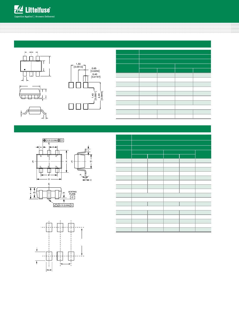
Package Dimensions — SC70-6
Package
SC70-6
Pins
6
JEDEC
MO-203
Millimeters
Inches
Min
Max
Min
Max
A
0.80
1.10
0.031
0.043
A1
0.00
0.10
0.000
0.004
A2
0.70
1.00
0.028
0.039
B
0.15
0.30
0.006
0.012
c
0.08
0.25
0.003
0.010
D
1.85
2.25
0.073
0.089
E
1.15
1.35
0.045
0.053
e
0.65 BSC
0.026 BSC
HE
2.00
2.40
0.079
0.094
L
0.26
0.46
0.010
0.018
D
A2 A
A1
C
L
E
HE
2
1
3
6
5
4
e
e
B
Solder Pad Layout
Package Dimensions — SOT23-6
Package
SOT23-6
Pins
6
JEDEC
MO-178
Millimeters
Inches
Notes
Min
Max
Min
Max
A
0.900
1.450
0.035
0.057
-
A1
0.000
0.150
0.000
0.006
-
A2
0.900
1.300
0.035
0.051
-
b
0.350
0.500
0.0138
0.0196
-
C
0.080
0.220
0.0031
0.009
-
D
2.800
3.000
0.11
0.118
3
E
2.600
3.000
0.102
0.118
-
E1
1.500
1.750
0.06
0.069
3
e
0.95 Ref
0.0374 Ref
-
e1
1.9 Ref
0.0748 Ref
-
L
0.100
0.600
0.004
0.023
4,5
N
6
6
6
a
0º
10º
0º
10º
-
M
2.590
0.102
-
O
0.690
.027 TYP
-
P
0.990
.039 TYP
-
R
0.950
0.038
-
O
P
R
M
Recommended Solder Pad Layout
Notes:
1. Dimensioning and tolerances per ANSI 14.5M-1982.
2. Package conforms to EIAJ SC-74 (1992).
3. Dimensions D and E1 are exclusive of mold flash, protrusions, or gate burrs.
4. Footlenth L measured at reference to seating plane.
5. “L” is the length of flat foot surface for soldering to substrate.
6. “N” is the number of terminal positions.
7. Controling dimension: MILLIMETER. Converted inch dimensions are not necessarily
exact.