Tvs diode array s, Tvs diode arrays, Lightning surge protection - sp03a-3.3 series – Littelfuse SP03A-3.3 Series User Manual
Page 4: Lightning surge protection - sp03-3.3 series, Family of products), Family of products) sp03a -3.3
©2012 Littelfuse, Inc.
Specifications are subject to change without notice.
Please refer to
www.littelfuse.com/SPA
for current information.
134
TVS Diode Array
Revision: March 20, 2012
SP03A-3.3 Series
TVS Diode Array
TVS Diode Arrays
(SPA
™
Family of Products)
SP03A
-3.3
Lightning Surge Protection - SP03A-3.3 Series
Part Numbering System
Product Characteristics
Ordering Information
Part Number
Package
Marking
Min. Order Qty.
SP03A-
3.3BTG
SOIC Tape & Reel
SP03A-3.3
2500
Lead Plating
Matte Tin
Lead Material
Copper Alloy
Lead Coplanarity
0.004 inches (0.102mm)
Substitute Material
Silicon
Body Material
Molded Epoxy
Flammability
UL 94 V-0
SP 03A 3.3 B T G
Series
Working
Voltage
Package
T= Tape & Reel
G= Green
–
B = SOIC
Silicon Protection
Array (SPA
TM
)
Family of
TVS Diode Arrays
Part Marking System
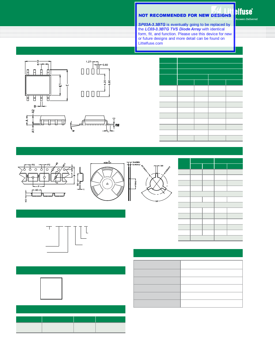
Package Dimensions — Mechanical Drawings and Recommended Solder Pad Outline
Package
SOIC
Pins
8
JEDEC
MS-012
Millimetres
Inches
Min
Max
Min
Max
A
1.35
1.75
0.053
0.069
A1
0.10
0.25
0.004
0.010
A2
1.25
1.65
0.050
0.065
B
0.31
0.51
0.012
0.020
c
0.17
0.25
0.007
0.010
D
4.80
5.00
0.189
0.197
E
5.80
6.20
0.228
0.244
E1
3.80
4.00
0.150
0.157
e
1.27 BSC
0.050 BSC
L
0.40
1.27
0.016
0.050
o
Recommended
Soldering Pad Outline
(Reference Only)
F
L
First Line: Part number
Second Line: Date code
F
L
SP03A-3.3
XXXXXXXX
Notes :
1. All dimensions are in millimeters
2. Dimensions include solder plating.
3. Dimensions are exclusive of mold flash & metal burr.
4. Blo is facing up for mold and facing down for trim/form, i.e. reverse trim/form.
5. Package surface matte finish VDI 11-13.
Embossed Carrier Tape & Reel Specification — SOIC Package
Millimetres
Inches
Min
Max
Min
Max
E
1.65
1.85
0.065
0.073
F
5.4
5.6
0.213
0.22
P2
1.95
2.05
0.077
0.081
D
1.5
1.6
0.059
0.063
D1
1.50 Min
0.059 Min
P0
3.9
4.1
0.154
0.161
10P0
40.0 +/- 0.20
1.574 +/- 0.008
W
11.9
12.1
0.468
0.476
P
7.9
8.1
0.311
0.319
A0
6.3
6.5
0.248
0.256
B0
5.1
5.3
0.2
0.209
K0
2
2.2
0.079
0.087
t
0.30 +/- 0.05
0.012 +/- 0.002