Littelfuse P6SMB Series User Manual
P6smb series, Transient voltage suppression diodes, Surface mount – 600w > p6smb series
Transient Voltage Suppression Diodes
© 2014 Littelfuse, Inc.
Specifications are subject to change without notice.
Revised: 01/20/14
Surface Mount – 600W > P6SMB series
Agency Approvals
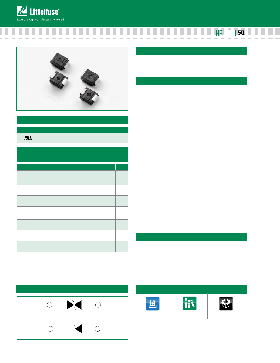
Description
The P6SMB series is designed specifically to protect
sensitive electronic equipment from voltage transients
induced by lightning and other transient voltage events.
Features
• Excellent clamping
capability
• Low incremental surge
resistance
• Typical I
R
less than 1µA
above 12V
• For surface mounted
applications to optimize
board space
• Low profile package
• Typical failure mode is
short from over-specified
voltage or current
• Whisker test is conducted
based on JEDEC
JESD201A per its table 4a
and 4c
• IEC-61000-4-2 ESD
15kV(Air), 8kV (Contact)
• ESD protection of data
lines in accordance with
IEC 61000-4-2 (IEC801-2)
• EFT protection of data
lines in accordance with
IEC 61000-4-4 (IEC801-4)
• Built-in strain relief
• 600W peak pulse power
capability at 10/1000μs
waveform, repetition rate
(duty cycles):0.01%
• Fast response time:
typically less than 1.0ps
from 0V to BV min
•
V
BR
@T
J
= V
BR
@25°C × (1+
α
T
x (T
J
- 25))
(αT: Temperature Coefficient)
• Glass passivated chip
junction
• High temperature
soldering guaranteed:
260°C/40 seconds at
terminals
• Plastic package has
underwriters laboratory
flammability 94V-O
• Meet MSL level1, per
J-STD-020, LF maximum
peak of 260°C
• Matte tin lead–free plated
• Halogen free and RoHS
compliant
Applications
TVS devices are ideal for the protection of I/O Interfaces,
V
CC
bus and other vulnerable circuits used in Telecom,
Computer, Industrial and Consumer electronic applications.
Maximum Ratings and Thermal Characteristics
(T
A
=25°C unless otherwise noted)
Parameter
Symbol
Value
Unit
Peak Pulse Power Dissipation at
T
A
=25ºC by 10/1000µs Waveform
(Fig.2)(Note 1), (Note 2)
P
PPM
600
W
Power Dissipation on Infinite Heat
Sink at T
A
=50°C
P
M(AV)
5.0
W
Peak Forward Surge Current, 8.3ms
Single Half Sine Wave (Note 3)
I
FSM
100
A
Maximum Instantaneous Forward
Voltage at 50A for Unidirectional
Only (Note 4)
V
F
3.5V/5.0
V
Operating Junction and Storage
Temperature Range
T
J
, T
STG
-55 to 150
°C
Typical Thermal Resistance Junction
to Lead
R
uJL
20
°C/W
Typical Thermal Resistance Junction
to Ambient
R
uJA
100
°C/W
Notes:
1. Non-repetitive current pulse , per Fig. 4 and derated above T
A
= 25°C per Fig. 3.
2. Mounted on copper pad area of 0.2x0.2” (5.0 × 5.0mm) to each terminal.
3. Measured on 8.3ms single half sine wave or equivalent square wave for unidirectional
device only,duty cycle=4 per minute maximum.
4. V
F
<3.5V for V
BR
_
<
200V and V
F
<5.0V for V
BR
_
>
201V.
AGENCY
AGENCY FILE NUMBER
E230531
RoHS
P6SMB Series
Bi-directional
Uni-directional
Functional Diagram
Bi-directional
Uni-directional
Cathode
Anode
Additional Information