Rainbow Electronics MAX159 User Manual
Page 9
Selecting Clock Mode
To start the conversion process on the MAX157/
MAX159, pull CS/SHDN low. At CS/SHDN’s falling
edge, the part wakes up, the internal T/H enters track
mode, and a conversion begins. In addition, the state of
SCLK at CS/SHDN’s falling edge selects internal (SCLK
= high) or external (SCLK = low) clock mode.
Internal Clock (f
SCLK
< 100kHz or f
SCLK
> 2.17MHz)
In internal clock mode, the MAX157/MAX159 run from
an internal, laser-trimmed oscillator to within 20% of the
2MHz specified clock rate. This releases the system
microprocessor from running the SAR conversion clock
and allows the conversion results to be read back at the
processor’s convenience, at any clock rate from 0 to
5MHz. Operating the MAX157/MAX159 in internal clock
mode is necessary for serial interfaces operating with
clock frequencies lower than 100kHz or greater than
2.17MHz. Select internal clock mode (Figure 5) by hold-
ing SCLK high during a high/low transition of CS/SHDN.
The first SCLK falling edge samples the data and initi-
ates a conversion using the integrated on-chip oscilla-
tor. After the conversion, the oscillator shuts off and
DOUT goes high, signaling the end of conversion
(EOC). Data can then be read out with SCLK.
External Clock (f
SCLK
= 100kHz to 2.17MHz)
External clock mode (Figure 6) is selected by transition-
ing CS/SHDN from high to low while SCLK is low. The
external clock signal not only shifts data out, but also
drives the analog-to-digital conversion. The input is
sampled and conversion begins on the falling edge of
the second clock pulse. Conversion must be completed
within 140µs to prevent degradation in the conversion
results caused by droop on the T/H capacitors. External
clock mode provides the best throughput for clock fre-
quencies between 100kHz and 2.17MHz.
MAX157/MAX159
+2.7V, Low-Power, 2-Channel,
108ksps, Serial 10-Bit ADCs in 8-Pin µMAX
_______________________________________________________________________________________
9
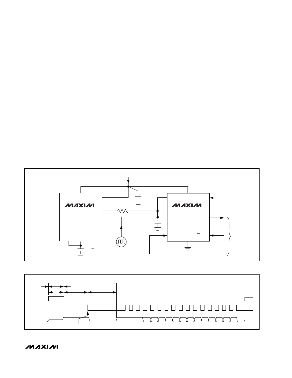
Figure 4. Analog Input with Anti-Aliasing Filter Structure
DOUT
D7
D8
MSB
CHID
1
1
EOC
SAMPLING INSTANT
HIGH-Z
D6
D5
D4
D3
D2
D1
D0
S1
S0
HIGH-Z
SCLK
6
7
8
9
10
11
1
2
3
4
5
12
13
14
15
16
t
CONV
t
WAKE
(t
ACQ
)
t
CS
POWER
DOWN
ACTIVE
ACTIVE
CS/SHDN
Figure 5. Internal Clock Mode Timing
SHDN
OUT
2
CLK
REF
EXTERNAL
REFERENCE
CS/SHDN
DOUT
2
3
8
4
µ
P/
µ
C
MAX7410
MAX7414
CH0
V
DD
V
DD
V
DD
GND
OS
GND
COM
0.01
µ
F
0.1
µ
F
470
Ω
0.01
µ
F
CH1
IN
f
CORNER
= 15kHz
7
4
5
5
7
6
8
1
1
6
3
SCLK
MAX157
1.5MHz
CLOCK