Rainbow Electronics MAX159 User Manual
Page 12
MAX157/MAX159
QSPI Interface
Using the high-speed QSPI interface with CPOL = 0
and CPHA = 0, the MAX157/MAX159 supports a maxi-
mum f
SCLK
of 2.17MHz. The QSPI circuit in Figure 9a
can be programmed to perform a conversion on each
of the two channels for the MAX157.
Figure 9b shows the QSPI interface timing.
PIC16 with SSP Module
and PIC17 Interface
The MAX157/MAX159 are compatible with a PIC16/
PIC17 microcontroller (µC), using the synchronous seri-
al port (SSP) module.
To establish SPI communication, connect the controller
as shown in Figure 10a and configure the PIC16/PIC17
as system master by initializing its synchronous serial
port control register (SSPCON) and synchronous serial
port status register (SSPSTAT) to the bit patterns shown
in Tables 2 and 3.
In SPI mode, the PIC16/PIC17 µCs allow eight bits of
data to be synchronously transmitted and received
simultaneously. Two consecutive 8-bit readings (Figure
10b) are necessary to obtain the entire 10-bit result
from the ADC. DOUT data transitions on the serial
clock’s falling edge and is clocked into the µC on
SCLK’s rising edge. The first 8-bit data stream contains
three leading ones, the channel identification, and the
first four data bits starting with the MSB. The second 8-
bit data stream contains the remaining bits, D5 through
D0, and the two sub-bits S1 and S0.
Layout, Grounding, and Bypassing
For best performance use printed circuit boards
(PCBs), wire-wrap configurations are not recommend-
ed, since the layout should ensure proper separation of
analog and digital traces. Run analog and digital lines
anti-parallel to each other, and don’t layout digital sig-
nal paths underneath the ADC package. Use separate
analog and digital PCB ground sections with only one
+2.7V, Low-Power, 2-Channel,
108ksps, Serial 10-Bit ADCs in 8-Pin µMAX
12
______________________________________________________________________________________
HIGH-Z
SAMPLING
INSTANT
D9
CHID
D8
D7
D6
D5
1
2
3
4
5
6
7
8
10
9
11
12
13
14
15
16
D4
D3
D2
D1
D0
S0
S1
DOUT*
CS/SHDN
SCLK
1ST BYTE READ
2ND BYTE READ
MSB
LSB
*WHEN CS/SHDN IS HIGH, DOUT = HIGH -Z
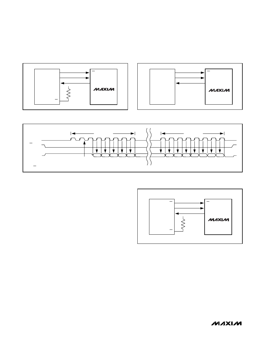
Figure 8c. SPI/MICROWIRE Interface Timing Sequence (CPOL = CPHA = 0)
CS/SHDN
SCLK
DOUT
CS
SCK
MISO
V
DD
SS
QSPI
MAX157
MAX159
Figure 9a. QSPI Connections
MAX157
MAX159
CS/SHDN
SCLK
DOUT
I/O
SK
SI
MICROWIRE
CS/SHDN
SCLK
DOUT
I/O
SCK
MISO
V
DD
SS
SPI
MAX157
MAX159
Figure 8a. SPI Connections
Figure 8b. MICROWIRE Connections