Rainbow Electronics MAX159 User Manual
Page 11
etc. Therefore, SNR is computed by taking the ratio of
the RMS signal to the RMS noise (which includes all
spectral components minus the fundamental), the first
five harmonics, and the DC offset.
Signal-to-Noise Plus Distortion (SINAD)
Signal-to-noise plus distortion is the ratio of the funda-
mental input frequency’s RMS amplitude to RMS equiv-
alent of all other ADC output signals:
Effective Number of Bits (ENOB)
ENOB indicates the global accuracy of an ADC at a
specific input frequency and sampling rate. An ideal
ADC’s error consists of quantization noise only. With an
input range equal to the full-scale range of the ADC,
calculate the effective number of bits as follows:
ENOB = (SINAD - 1.76) / 6.02
Total Harmonic Distortion (THD)
THD is the ratio of the RMS sum of the first five harmon-
ics of the input signal to the fundamental itself. This is
expressed as:
where V
1
is the fundamental amplitude and V
2
through
V
5
are the amplitudes of the 2nd through 5th-order har-
monics.
Spurious-Free Dynamic Range (SFDR)
SFDR is the ratio of RMS amplitude of the fundamental
(maximum signal component) to the RMS value of the
next largest spurious component, excluding DC offset.
Connection to Standard Interfaces
The MAX157/MAX159 interface is fully compatible with
SPI/QSPI and MICROWIRE standard serial interfaces.
If a serial interface is available, establish the CPU’s seri-
al interface as master so that the CPU generates the
serial clock for the MAX157/MAX159. Select a clock fre-
quency from 100kHz to 2.17MHz (external clock mode).
1) Use a general-purpose I/O line on the CPU to pull
CS/SHDN low while SCLK is low.
2) Wait for the minimum wake-up time (t
WAKE
) speci-
fied before activating SCLK.
3) Activate SCLK for a minimum of 16 clock cycles. The
first falling clock edge will generate a serial data-
stream of three leading ones, followed by the chan-
nel identification, the MSB of the digitized input
signal, and two sub-bits. DOUT transitions on
SCLK’s falling edge and is available in MSB-first for-
mat. Observe the SCLK to DOUT valid timing char-
acteristic. Data should be clocked into the µP on
SCLK’s rising edge.
4) Pull CS/SHDN high at or after the 16th falling clock
edge. If CS/SHDN remains low, trailing zeros will be
clocked out after the sub-bits.
5) With CS/SHDN high, wait at least 60ns (t
CS
), before
starting a new conversion by pulling CS/SHDN low.
A conversion can be aborted by pulling CS/SHDN
high before the conversion ends; wait at least 60ns
before starting a new conversion.
Data can be output either in two 8-bit sequences or
continuously. The bytes will contain the result of the
conversion padded with three leading ones, the chan-
nel identification before the MSB, and two trailing sub-
bits. If the serial clock hasn’t been idled after the last
sub-bit (S0) and CS/SHDN is kept low, DOUT sends
trailing zeros.
SPI and MICROWIRE Interface
When using SPI (Figure 8a) or MICROWIRE (Figure 8b)
interfaces, set CPOL = 0 and CPHA = 0. Conversion
begins with a falling edge on CS/SHDN (Figure 8c). Two
consecutive 8-bit readings are necessary to obtain the
entire 10-bit result from the ADC. DOUT data transitions
on the serial clock’s falling edge and is clocked into the
µP on SCLK’s rising edge. The first 8-bit data stream
contains three leading ones, followed by channel identi-
fication and the first four data bits starting with the MSB.
The second 8-bit data stream contains the remaining
bits, D5 through D0, and the sub-bits S1 and S0.
THD = 20 log
V
+ V
+ V
+ V
V
22
32
42
52
12
⋅
(
)
SINAD(dB) = 20 log
Signal
(Noise + Distortion)
RMS
RMS
⋅
MAX157/MAX159
+2.7V, Low-Power, 2-Channel,
108ksps, Serial 10-Bit ADCs in 8-Pin µMAX
______________________________________________________________________________________
11
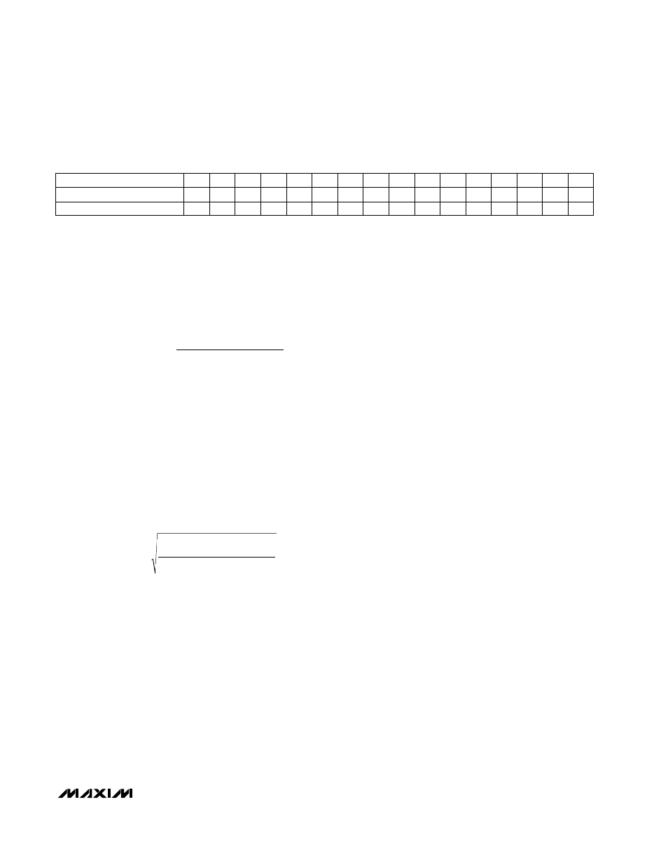
Table 1. Serial Output Data Stream for Internal and External Clock Mode
D0
D1
D2
D3
D4
D5
D6
D7
D8
D9
CHID
1
1
EOC
DOUT (Internal Clock)
14
13
12
11
10
9
8
7
6
5
4
3
2
1
SCLK CYCLE
D0
D1
D2
D3
D4
D5
D6
D7
D8
D9
CHID
1
1
1
DOUT (External Clock)
S0
S1
S0
S1
16
15