Applications information – Rainbow Electronics MAX159 User Manual
Page 10
MAX157/MAX159
+2.7V, Low-Power, 2-Channel,
108ksps, Serial 10-Bit ADCs in 8-Pin µMAX
10
______________________________________________________________________________________
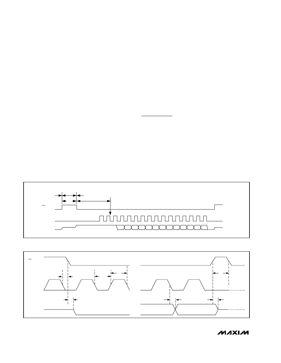
Output Data Format
Table 1 illustrates the 16-bit, serial data-stream output
format for both the MAX157 and MAX159. The first three
bits are always logic high (including the EOC bit for
internal clock mode), followed by the channel identifica-
tion (CHID = 0 for CH0, CHID = 1 for CH1, CHID = 1 for
MAX159), the 10 bits of data in MSB first format, and
two sub-LSB bits (S1 and S0). After the last bit has been
read out, additional SCLK pulses will clock out trailing
zeros. DOUT transitions on the falling edge of SCLK.
The output remains high impedance when CS/SHDN is
high.
External Reference
An external reference is required for both the MAX157
and MAX159. At REF, the DC input resistance is a mini-
mum of 18k
Ω
. During a conversion, a reference must
be able to deliver 250µA of DC load current and have
an output impedance of 10
Ω
or less. Use a 0.1µF
bypass capacitor for best performance. The reference
input structure allows a voltage range of 0 to (V
DD
+
50mV) although noise levels will decrease effective res-
olution at lower reference voltages.
Automatic Power-Down Mode
Whenever the MAX157/MAX159 are not selected
(CS/SHDN = V
DD
), the parts enter their shutdown mode.
In shutdown all internal circuitry is turned off, which
reduces the supply current to typically less than 0.2µA.
With an external reference stable to within 1LSB, the
wake-up time is 2.5µs. If the external reference is not sta-
ble within 1LSB, the wake-up time must be increased to
allow the reference to stabilize.
Applications Information
Signal-to-Noise Ratio (SNR)
For a waveform perfectly reconstructed from digital
samples, SNR is the ratio of full-scale analog input
(RMS value) to the RMS quantization error (residual
error). The ideal, theoretical minimum analog-to-digital
noise is caused by quantization error only and results
directly from the ADC’s resolution (N bits):
SNR
(MAX)
= (6.02
·
N + 1.76)dB
In reality, there are other noise sources besides quanti-
zation noise: thermal noise, reference noise, clock jitter,
DOUT
D7
D8
MSB
CHID
SAMPLING INSTANT
HIGH-Z
D6
D5
D4
D3
D2
D1
D0
S1
S0
HIGH-Z
SCLK
6
7
8
9
10
11
1
2
3
4
5
12
13
14
15
16
t
WAKE
(t
ACQ
)
t
CS
POWER
DOWN
ACTIVE
ACTIVE
CS/SHDN
Figure 6. External Clock Mode Timing
• • •
• • •
• • •
CS/SHDN
SCLK
DOUT
t
CL
t
DV
HIGH-Z
HIGH-Z
t
CH
t
CS
t
DO
t
TR
t
SCLKS
Figure 7. Detailed Serial-Interface Timing Sequence