Rainbow Electronics MAX159 User Manual
Page 8
MAX157/MAX159
+2.7V, Low-Power, 2-Channel,
108ksps, Serial 10-Bit ADCs in 8-Pin µMAX
8
_______________________________________________________________________________________
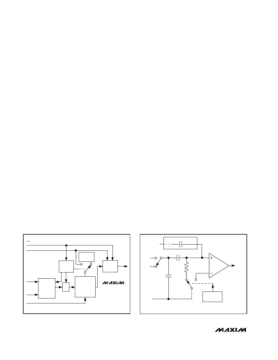
The capacitive digital-to-analog converter (DAC)
adjusts during the remainder of the conversion cycle
to restore node ZERO to 0V within the limits of 10-bit
resolution. This action is equivalent to transferring a
16pF
·
[(V
IN
+) - (V
IN
-)] charge from C
HOLD
to the bina-
ry-weighted capacitive DAC, which in turn forms a digi-
tal representation of the analog input signal.
Track/Hold
The ADC’s T/H stage enters its tracking mode on the
falling edge of CS/SHDN. For the MAX157 (single-
ended inputs), IN- is connected to GND and the con-
verter samples the positive (“+”) input. For the MAX159
(pseudo-differential inputs), IN- connects to the nega-
tive input (“-”), and the difference of [(V
IN
+) - (V
IN
-)] is
sampled. At the end of the conversion, the positive
input connects back to IN+ and C
HOLD
charges to the
input signal.
The time required for the T/H stage to acquire an input
signal is a function of how fast its input capacitance is
charged. If the input signal’s source impedance is high,
the acquisition time lengthens and more time must be
allowed between conversions. The acquisition time,
t
ACQ
, is the maximum time the device takes to acquire
the signal, and is also the minimum time required for
the signal to be acquired. Calculate this with the follow-
ing equation:
t
ACQ
= 7(R
S
+ R
IN
)C
IN
where R
S
is the source impedance of the input signal,
R
IN
(9k
Ω
) is the input resistance, and C
IN
(16pF) is the
input capacitance of the ADC. Source impedances
below 4k
Ω
have no significant impact on the AC perfor-
mance of the MAX157/MAX159.
Higher source impedances can be used if a 0.01µF
capacitor is connected to the individual analog inputs.
Together with the input impedance, this capacitor forms
an RC filter, limiting the ADC’s signal bandwidth.
Input Bandwidth
The MAX157/MAX159 T/H stage offers both a 2.25MHz
small-signal and a 1MHz full-power bandwidth, which
makes it possible to use the parts for digitizing high-
speed transients and measuring periodic signals with
bandwidths exceeding the ADC’s sampling rate by
using undersampling techniques. To avoid high-fre-
quency signals being aliased into the frequency band
of interest, anti-alias filtering is recommended. Most
aliasing problems can be fixed easily with an external
resistor and a capacitor. However, if DC precision is
required, it is usually best to choose a continuous
or switched-capacitor filter, such as the MAX7410/
MAX7414 (Figure 4). Their Butterworth characteristic
generally provides the best compromise (with regard to
rolloff and attenuation) in filter configurations, is easy to
design, and provides a maximally flat passband re-
sponse.
Analog Input Protection
Internal protection diodes, which clamp the analog
input to V
DD
and GND, allow each input channel to
swing within GND - 300mV to V
DD
+ 300mV without
damage. However, for accurate conversions both
inputs must not exceed V
DD
+ 50mV or be less than
GND - 50mV.
If an off-channel analog input voltage exceeds the
supplies, limit the input current to 4mA.
MAX157
MAX159
10+2 BIT
SAR
ADC
SCLK
IN
OUT
ANALOG
INPUT
MUX
(2 CHANNEL)
CH0
(CH+)
CH1
(CH-)
REF
( ) ARE FOR MAX159
T/H
CONTROL
LOGIC
SCLK
CS/SHDN
INTERNAL
CLOCK
OUTPUT
REGISTER
DOUT
Figure 2. MAX157/MAX159 Simplified Functional Diagram
CH0
(CH+)
CH1
(CH-)
GND
C
SWITCH
TRACK
T/H
R
IN
9k
HOLD
CAPACITIVE DAC
CONTROL
LOGIC
REF
ZERO
TO SAR
( ) ARE FOR MAX159
COMPARATOR
–
+
C
HOLD
16pF
SINGLE-ENDED MODE: CHO, CH1 = IN+; GND = IN-
DIFFERENTIAL MODE: CH+ = IN+; CH- = IN-
INPUT
MUX
Figure 3. Analog Input Channel Structure