Rainbow Electronics MAX159 User Manual
Page 13
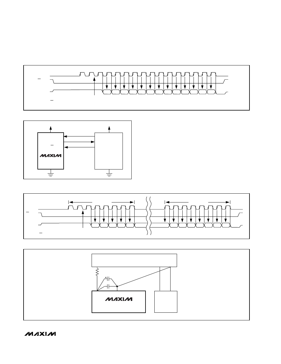
star-point (Figure 11) connecting the two ground sys-
tems (analog and digital). For lowest-noise operation,
ensure the ground return to the star ground’s power
supply is low impedance and as short as possible.
Route digital signals far away from sensitive analog and
reference inputs.
High-frequency noise in the power supply (V
DD
) could
influence the proper operation of the ADC’s fast com-
parator. Bypass V
DD
to the star ground with a network
of two parallel capacitors, 0.1µF and 1µF, located as
close as possible to the power supply pin of the
MAX157/MAX159. Minimize capacitor lead length for
best supply-noise rejection and add an attenuation
resistor (10
Ω
) if the power supply is extremely noisy.
MAX157/MAX159
+2.7V, Low-Power, 2-Channel,
108ksps, Serial 10-Bit ADCs in 8-Pin µMAX
______________________________________________________________________________________
13
SCK
SDI
GND
GND
I/O
SCLK
DOUT
CS/SHDN
V
DD
V
DD
MAX157
MAX159
PIC16/PIC17
CHID
D9
D8
D7
D6
1
2
3
4
5
6
7
8
9
10
11
12
13
14
15
16
D5
D4
D3
D2
D1
HIGH-Z
DOUT*
CS/SHDN
SCLK
1ST BYTE READ
2ND BYTE READ
SAMPLING INSTANT
*WHEN CS/SHDN IS HIGH, DOUT = HIGH - Z
MSB
LSB
D0
S1
S0
Figure 10b. SPI Interface Timing Sequence with PIC16/17 in Master Mode (CKE = 1, CKP = 0, SMP = 0, SSPM3–SSPM0 = 0001)
Figure 10a. SPI Interface Connection for a PIC16/PIC17
Controller
CHID
D9
D8
D7
D6
1
2
3
4
5
6
7
8
9
10
11
12
13
14
15
16
D5
D4
D3
D2
D1
HIGH-Z
DOUT
CS/SHDN
SCLK
SAMPLING INSTANT
*WHEN CS/SHDN IS HIGH, DOUT = HIGH - Z
MSB
LSB
D0
S1
S0
Figure 9b. QSPI Interface Timing Sequence (CPOL = CPHA = 0)
+3V
GND
+3V
POWER SUPPLIES
DGND
+3V
GND
V
DD
DIGITAL
CIRCUITRY
MAX157
MAX159
R* = 10
Ω
1
µ
F
0.1
µ
F
* OPTIONAL FILTER RESISTOR
Figure 11. Power-Supply Bypassing and Grounding