Electrical characteristics (continued), Timing characteristics (figure 7) – Rainbow Electronics MAX159 User Manual
Page 4
MAX157/MAX159
+2.7V, Low-Power, 2-Channel,
108ksps, Serial 10-Bit ADCs in 8-Pin µMAX
4
_______________________________________________________________________________________
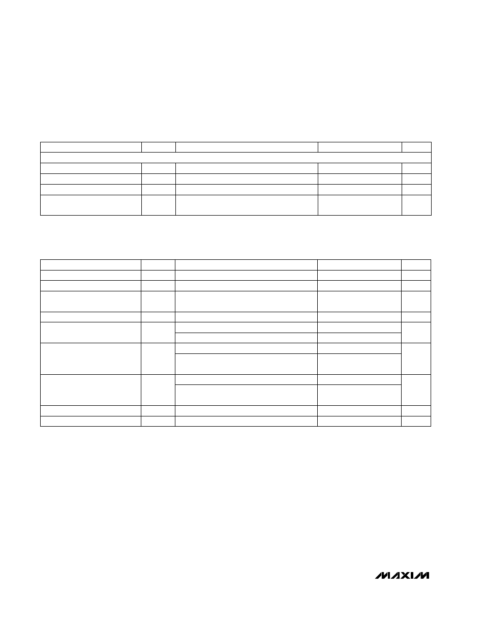
ELECTRICAL CHARACTERISTICS (continued)
(V
DD
= +2.7V to +5.25V, V
REF
= 2.5V, 0.1µF capacitor at REF, f
SCLK
= 2.17MHz, 16 clocks/conversion cycle (108ksps),
CH- = GND for MAX159, T
A
= T
MIN
to T
MAX
, unless otherwise noted. Typical values are at T
A
= +25°C.)
TIMING CHARACTERISTICS (Figure 7)
(V
DD
= +2.7V to +5.25V, V
REF
= 2.5V, 0.1µF capacitor at REF, f
SCLK
= 2.17MHz, 16 clocks/conversion cycle (108ksps),
CH- = GND for MAX159, T
A
= T
MIN
to T
MAX
, unless otherwise noted. Typical values are at T
A
= +25°C.)
Note 1:
Tested at V
DD
= +2.7V.
Note 2:
Relative accuracy is the deviation of the analog value at any code from its theoretical value after full-scale range has been
calibrated.
Note 3:
Offset nulled.
Note 4:
The on channel is grounded; the sine wave is applied to off channel (MAX157 only).
Note 5:
Conversion time is defined as the number of clock cycles times the clock period; clock has 50% duty cycle.
Note 6:
The common-mode range for the analog inputs is from GND to V
DD
(MAX159 only).
Note 7:
ADC performance is limited by the converter’s noise floor, typically 300µVp-p.
Note 8:
Guaranteed by design. Not subject to production testing.
Note 9:
Measured as V
FS
(2.7V) - V
FS
(5.25V).
PARAMETER
SYMBOL
MIN
TYP
MAX
UNITS
0
5
SCLK Clock Frequency
f
SCLK
0.1
2.17
MHz
SCLK Fall to Output Data Valid
t
DO
20
120
ns
215
CS/SHDN Fall to Output Enable
Wake-Up Time
t
WAKE
2.5
µs
t
DV
120
ns
CS/SHDN Rise to Output
Disable
t
TR
120
ns
SCLK Pulse Width High
t
CH
50
ns
CONDITIONS
Internal clock, SCLK for data transfer only
(Note 8)
Internal clock, SCLK for data transfer only
External clock
C
L
= 100pF
External clock
C
L
= 100pF (Figure 1)
C
L
= 100pF (Figure 1)
ns
SCLK to CS/SHDN Setup
t
SCLKS
60
CS/SHDN Pulse Width
t
CS
60
ns
215
SCLK Pulse Width Low
t
CL
50
ns
Internal clock, SCLK for data transfer only
(Note 8)
External clock
POWER REQUIREMENTS
Power-Supply Rejection
(Note 9)
PSR
±0.15
mV
V
DD
= 2.7V to 5.25V, full-scale input
PARAMETER
SYMBOL
MIN
TYP
MAX
UNITS
Positive Supply Voltage
V
DD
+2.7
+5.25
V
CONDITIONS
Positive Supply Current
I
DD
0.9
2.0
mA
Operating mode
Positive Supply Current
I
DD
0.2
5
µA
Shutdown, CS/SHDN = GND
POWER REQUIREMENTS