Standard application circuit, Detailed description – Rainbow Electronics MAX1637 User Manual
Page 7
MAX1637
Miniature, Low-Voltage,
Precision Step-Down Controller
_______________________________________________________________________________________
7
MAX1637
0.1
µ
F
V
BIAS
+5V
NOMINAL
0.1
µ
F
1
µ
F
470pF
C1
Q1
CMPSH-3
Q2
C2
L1
*
R1
R2
R3
OUTPUT
4.7
µ
F
*SEE
RECTIFIER CLAMP DIODE SECTION
**OPTIONAL RC NETWORK FOR POWER-ON-RESET
DL
PGND
LX
DH
BST
V
GG
V
CC
V
BATT
CSH
CSL
FB
1M
**
ON/OFF
CC
GND
SHDN
REF
SYNC
20
Ω
SKIP
0.01
µ
F
**
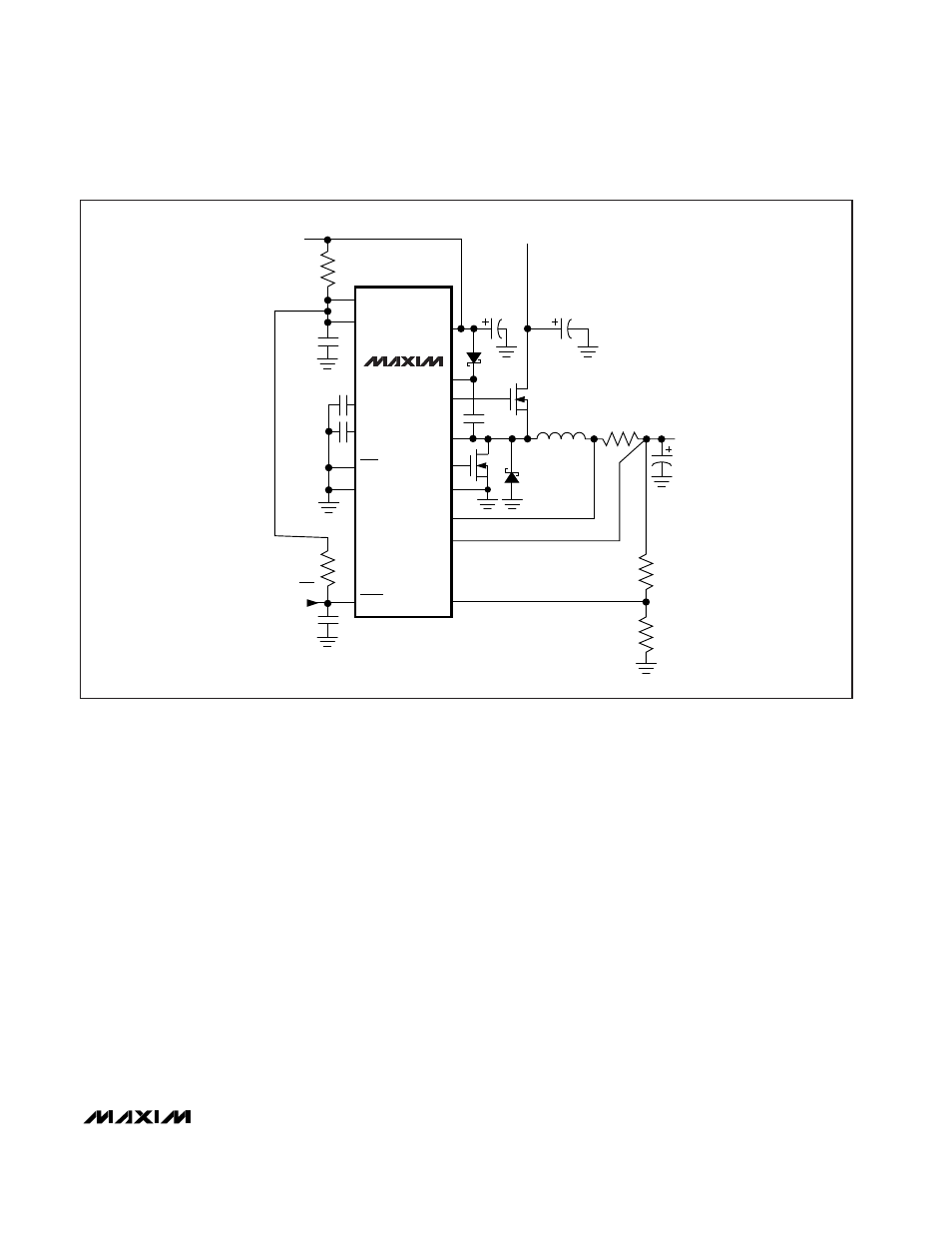
Figure 1. Standard Application Circuit
______Standard Application Circuit
The basic MAX1637 buck converter (Figure 1) is easily
adapted to meet a wide range of applications where a
5V or lower supply is available. The components listed
in Table 1 represent a good set of trade-offs among
cost, size, and efficiency, while staying within the worst-
case specification limits for stress-related parameters
such as capacitor ripple current. Do not change the cir-
cuit’s switching frequency without first recalculating
component values (particularly inductance value at
maximum battery voltage).
The power Schottky diode across the synchronous rec-
tifier is optional because the MOSFETs chosen incorpo-
rate a high-speed silicon diode. However, installing the
Schottky will generally improve efficiency by about 1%.
If used, the Schottky diode DC current must be rated to
at least one-third of the maximum load current.
_______________Detailed Description
The MAX1637 is a BiCMOS, switch-mode power-supply
(SMPS) controller designed primarily for buck-topology
regulators in battery-powered applications where high
efficiency and low quiescent supply current are critical.
Light-load efficiency is enhanced by automatic idle-
mode operation—a variable-frequency, pulse-skipping
mode that reduces transition and gate-charge losses.
The step-down, power-switching circuit consists of two
N-channel MOSFETs, a rectifier, and an LC output filter.
Output voltage for this device is the average AC volt-
age at the switching node, which is regulated by
changing the duty cycle of the MOSFET switches. The
gate-drive signal to the high-side N-channel MOSFET,
which must exceed the battery voltage, is provided by
a flying-capacitor boost circuit that uses a 100nF
capacitor between BST and LX. Figure 2 shows the
major circuit blocks.