Rainbow Electronics MAX1637 User Manual
Page 12
MAX1637
Miniature, Low-Voltage,
Precision Step-Down Controller
12
______________________________________________________________________________________
REF, V
CC
, and V
GG
Supplies
The 1.100V reference (REF) is accurate to ±2% over
temperature, making REF useful as a precision system
reference. Bypass REF to GND with a 0.22µF (min)
capacitor. REF can supply up to 50µA for external
loads. Loading REF reduces the main output voltage
slightly because of the reference load-regulation error.
The MAX1637 has two independent supply pins, V
CC
and V
GG
. V
CC
powers the sensitive analog circuitry of
the SMPS, while V
GG
powers the high-current MOSFET
drivers. No protection diodes or sequencing require-
ments exist between the two supplies. Isolate V
GG
from
V
CC
with a 20
Ω
resistor if they are powered from the
same supply. Bypass V
CC
to GND with a 0.1µF capaci-
tor located directly adjacent to the pin. Use only small-
signal diodes for the boost circuit (10mA to 100mA
Schottky or 1N4148 diodes are preferred), and bypass
V
GG
to PGND with a 4.7µF capacitor directly at the
package pins. The V
CC
and V
GG
input range is 3.15V
to 5.5V.
High-Side Boost Gate Drive (BST)
Gate-drive voltage for the high-side N-channel switch is
generated by a flying-capacitor boost circuit (Figure 2).
The capacitor between BST and LX is alternately
charged from the V
GG
supply and placed parallel to
the high-side MOSFET’s gate-source terminals.
On start-up, the synchronous rectifier (low-side
MOSFET) forces LX to 0V and charges the boost
capacitor to V
GG
. On the second half-cycle, the SMPS
turns on the high-side MOSFET by closing an internal
switch between BST and DH. This provides the neces-
sary enhancement voltage to turn on the high-side
switch, an action that boosts the gate-drive signal
above the battery voltage.
Ringing at the high-side MOSFET gate (DH) in discon-
tinuous-conduction mode (light loads) is a natural oper-
ating condition. It is caused by residual energy in the
tank circuit, formed by the inductor and stray capaci-
tance at the switching node, LX. The gate-drive nega-
tive rail is referred to LX, so any ringing there is directly
coupled to the gate-drive output.
Synchronous-Rectifier Driver (DL)
Synchronous rectification reduces conduction losses in
the rectifier by shunting the normal Schottky catch
diode with a low-resistance MOSFET switch. Also, the
synchronous rectifier ensures proper start-up of the
boost gate-driver circuit. If the synchronous power
MOSFET is omitted for cost or other reasons, replace it
with a small-signal MOSFET, such as a 2N7002.
If the circuit is operating in continuous-conduction
mode, the DL drive waveform is simply the complement
of the DH high-side-drive waveform (with controlled
dead time to prevent cross-conduction or “shoot-
through”). In discontinuous (light-load) mode, the syn-
chronous switch is turned off as the inductor current
falls through zero.
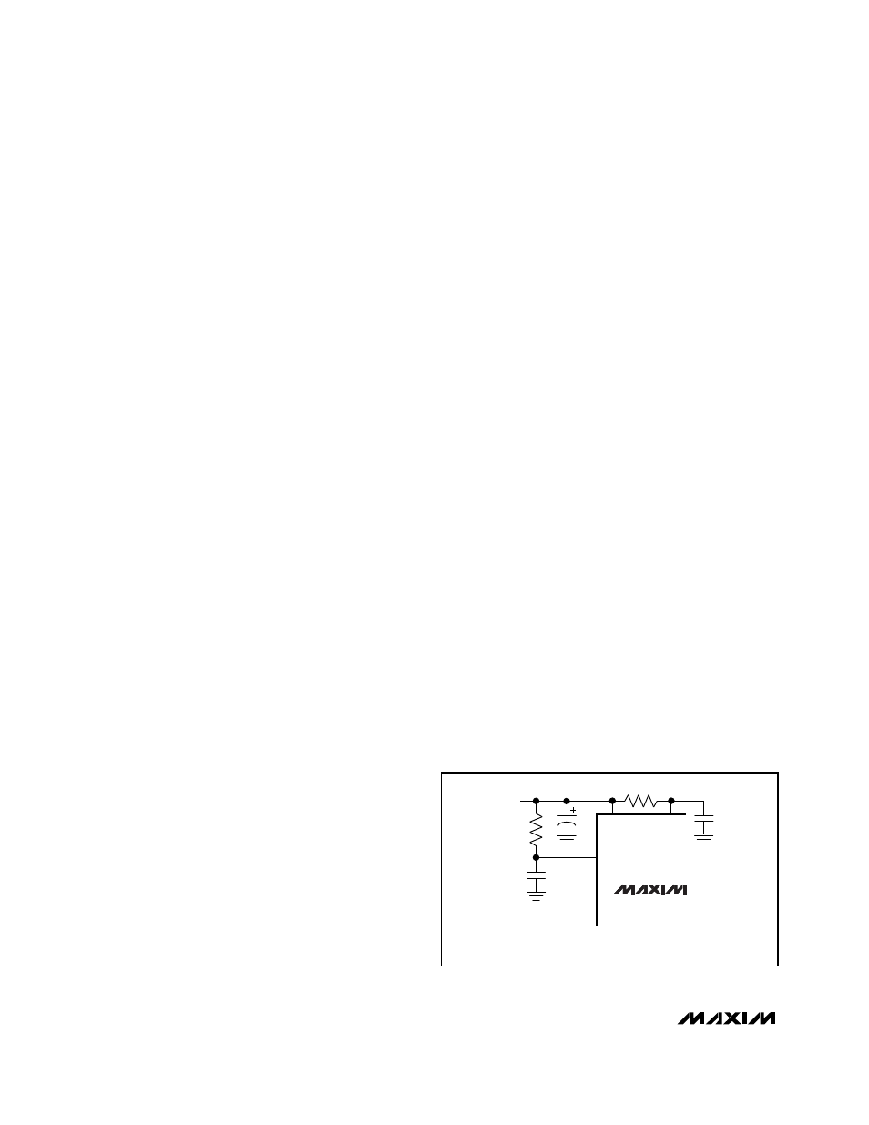
Shutdown Mode and Power-On Reset
SHDN is a logic input with a threshold of about 1.5V
that, when held low, places the IC in its 0.5µA shut-
down mode. The MAX1637 has no power-on-reset cir-
cuitry, and the state of the device is not known on initial
power-up. In applications that use logic to drive SHDN,
it may be necessary to toggle SHDN to initialize the
part once V
CC
is stable. In applications that require
automatic start-up, drive SHDN through an external RC
network (Figure 5). The network will hold SHDN low
until V
CC
stabilizes. Typical values for R and C are 1M
Ω
and 0.01µF. For slow-rising V
CC
, use a larger capacitor.
When cycling V
CC
, V
CC
must stay low long enough to
discharge the 0.01µF capacitor, otherwise the circuit
may not start. A diode may be added in parallel with
the resistor to speed up the discharge.
Current-Limiting and Current-
Sense Inputs (CSH and CSL)
The current-limit circuit resets the main PWM latch and
turns off the high-side MOSFET switch whenever the
voltage difference between CSH and CSL exceeds
100mV. This limiting is effective for both current flow
directions, putting the threshold limit at ±100mV. The
tolerance on the positive current limit is ±20%, so the
external low-value sense resistor (R1) must be sized for
80mV / I
PEAK
, where I
PEAK
is the peak inductor current
required to support the full load current. Components
must be designed to withstand continuous current
stresses of 120mV / R1.
MAX1637
SHDN
R = 1M
Ω
C = 0.01
µ
F
V
IN
V
GG
C
R
V
CC
Figure 5. Power-On Reset RC Network for Automatic Start-Up