Typical operating characteristics (continued), Pin description – Rainbow Electronics MAX1637 User Manual
Page 6
MAX1637
Miniature, Low-Voltage,
Precision Step-Down Controller
6
_______________________________________________________________________________________
____________________________________Typical Operating Characteristics (continued)
(V
OUT
= 3.3V, T
A
= +25°C, unless otherwise noted.)
500
µ
s/div
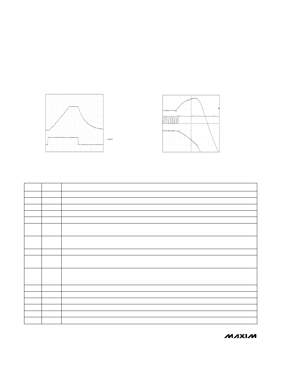
TIME EXITING SHUTDOWN
(V
OUT
= 3.3V, I
LOAD
= 7A)
MAX1637-16
V
OUT
1V/div
V
SHDN
5V/div
V
OUT
100mV/div
V
DL
INDUCTOR
CURRENT
-5A
0A
0V
5V
-10A
OVERVOLTAGE-PROTECTION WAVEFORMS
(V
IN
SHORTED TO V
OUT
THROUGH A 0.5
Ω
RESISTOR)
MAX1637-17
10
µ
s/div
______________________________________________________________Pin Description
PIN
High-Side Current-Sense Input
CSH
1
FUNCTION
NAME
Low-Side Current-Sense Input
CSL
2
Compensation Pin. Connect a small capacitor to GND to set the integration time constant.
CC
4
Feedback Input. Connect to center of resistor divider.
FB
3
Shutdown Control Input. Turns off entire IC. When low, reduces supply current below 0.5µA (typ). Drive with
logic input or connect to RC network between GND and V
CC
for automatic start-up.
SHDN
6
Analog Ground
GND
8
Oscillator Frequency Select and Synchronization Input. Tie to V
CC
for 300kHz operation; tie to GND for
200kHz operation.
SYNC
7
1.100V Reference Output. Capable of sourcing 50µA for external loads. Bypass with 0.22µF minimum.
REF
5
Gate-Drive and Boost-Circuit Power Supply. Can be driven from a supply other than V
CC
. If the same supply
is used by both V
CC
and V
GG
, isolate V
CC
from V
GG
with a 20
Ω
resistor. Bypass to PGND with a 4.7µF
capacitor. V
GG
current = (Q
G1
+ Q
G2
) x f, where Q
G
is the MOSFET gate charge at V
GS
= V
GG
.
V
GG
10
Power Ground
PGND
12
Low-Side Gate-Driver Output
DL
11
High-Side Gate-Driver Output
DH
14
Low-Noise Mode Control. Forces fixed-frequency PWM operation when high.
SKIP
16
Inductor Connection
LX
15
Boost Capacitor Connection
BST
13
Main Analog Supply-Voltage Input to the Chip. V
CC
powers the PWM controller, logic, and reference. Input
range is 3.15V to 5.5V. Bypass to GND with a 0.1µF capacitor close to the pin.
V
CC
9