Chip information, Pin configuration – Rainbow Electronics MAX1844 User Manual
Page 21
Therefore, V
IN
must be greater than 3.13V, even with
very large output capacitance, and a practical input volt-
age with reasonable output capacitance would be 3.48V.
PC Board Layout Guidelines
Careful PC board layout is critical to achieving low
switching losses and clean, stable operation. The switch-
ing power stage requires particular attention (Figure 9). If
possible, mount all of the power components on the top
side of the board, with their ground terminals flush
against one another. Follow these guidelines for good
PC board layout:
• Keep the high-current paths short, especially at the
ground terminals. This practice is essential for stable,
jitter-free operation.
• Keep the power traces and load connections short.
This practice is essential for high efficiency. Using
thick copper PC boards (2oz vs. 1oz) can enhance
full-load efficiency by 1% or more. Correctly routing
PC board traces is a difficult task that must be
approached in terms of fractions of centimeters,
where a single milliohm of excess trace resistance
causes a measurable efficiency penalty.
• Minimize current sensing errors by connecting CS
directly to the R
SENSE
terminal.
• When trade-offs in trace lengths must be made, it is
preferable to allow the inductor charging path to be
made longer than the discharge path. For example,
it is better to allow some extra distance between the
input capacitors and the high-side MOSFET than to
allow distance between the inductor and the low-
side MOSFET or between the inductor and the out-
put filter capacitor.
• Route high-speed switching nodes (BST, LX, DH, and
DL) away from sensitive analog areas (REF, FB, CS).
Layout Procedure
1) Place the power components first, with ground termi-
nals adjacent (Q2 source, C
IN-
, C
OUT-
, D1 anode). If
possible, make all these connections on the top layer
with wide, copper-filled areas.
2) Mount the controller IC adjacent to MOSFET Q2,
preferably on the back side opposite Q2 in order to
keep LX, GND, and the DL gate-drive lines short and
wide. The DL gate trace must be short and wide,
measuring 10 to 20 squares (50 to 100 mils wide if the
MOSFET is 1 inch from the controller IC GND pin.
3) Group the gate-drive components (BST diode and
capacitor, V
DD
bypass capacitor) together near the
controller IC.
4) Make the DC-DC controller ground connections as
shown in Figure 9
.
This diagram can be viewed as
having two separate ground planes: power ground,
where all the high-power components go; and an ana-
log ground plane for sensitive analog components.
The analog ground plane and power ground plane
must meet only at a single point directly at the IC.
5) Connect the output power planes directly to the out-
put filter capacitor positive and negative terminals
with multiple vias. Place the entire DC-DC converter
circuit as close to the load as is practical.
MAX1844
High-Speed Step-Down Controller with
Accurate Current Limit for Notebook Computers
______________________________________________________________________________________
21
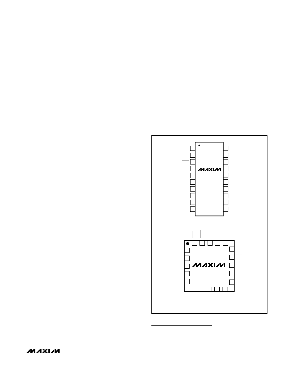
Chip Information
TRANSISTOR COUNT: 2963
PROCESS: BiCMOS
Pin Configuration
20
19
18
17
16
15
14
13
1
2
3
4
5
6
7
8
DH
LX
BST
SKIP
OVP
SHDN
LATCH
CS
TOP VIEW
V+
TON
V
CC
V
DD
REF
ILIM
OUT
FB
12
11
9
10
DL
GND
PGOOD
UVP
MAX1844EEP
20 QSOP
3
2
1
20
19
4
5
6
7
8
9
10
11
12
13
14
15
16
17
18
20 QFN
MAX1844EGP
V
CC
TON
V+
SKIP
BST
REF
ILIM
OUT
FB
OVP
LX
DH
CS
LATCH
SHDN
V
DD
DL
GND
PGOOD
UVP