Detailed description – Rainbow Electronics MAX1844 User Manual
Page 10
Detailed Description
The MAX1844 buck controller is targeted for low-voltage
power supplies for notebook computers. Maxim’s propri-
etary Quick-PWM pulse-width modulator in the MAX1844
is specifically designed for handling fast load steps while
maintaining a relatively constant operating frequency
and inductor operating point over a wide range of input
voltages. The Quick-PWM architecture circumvents the
poor load-transient timing problems of fixed-frequency
current-mode PWMs while also avoiding the problems
caused by widely varying switching frequencies in con-
ventional constant-on-time and constant-off-time PWM
schemes.
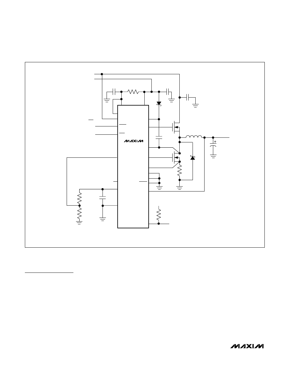
5V Bias Supply (V
CC
and V
DD
)
The MAX1844 requires an external 5V bias supply in
addition to the battery. Typically, this 5V bias supply is
the notebook’s 95% efficient 5V system supply. Keeping
the bias supply external to the IC improves efficiency
and eliminates the cost associated with the 5V linear reg-
ulator that would otherwise be needed to supply the
PWM circuit and gate drivers. If stand-alone capability is
needed, the 5V supply can be generated with an exter-
nal linear regulator such as the MAX1615.
The battery and 5V bias inputs can be connected
together if the input source is a fixed 4.5V to 5.5V supply.
If the 5V bias supply is powered up prior to the
MAX1844
High-Speed Step-Down Controller with
Accurate Current Limit for Notebook Computers
10
______________________________________________________________________________________
V
CC
UVP
V
IN
7V TO 20V
5V
BIAS SUPPLY
C2
330
µ
F
SEE TABLE 1 FOR OTHER COMPONENT SELECTIONS.
POWER-GOOD
INDICATOR
L1
4.7
µ
H
V
OUT
2.5V
SHDN
V+
D2
CMPSH-3
C6
3.3
µ
F
C7
0.1
µ
F
C4
0.22
µ
F
270k
Ω
130k
Ω
Q1
D1
R2
100k
Ω
Q2
R
SENSE
15m
Ω
C5
4.7
µ
F
R1
20
Ω
SKIP
ILIM
ON/OFF
CONTROL
LOW-NOISE
CONTROL
DL
LX
BST
DH
CS
OUT
FB
LATCH
OVP
PGOOD
V
DD
MAX1844
5V
TON
REF
GND
C1
10
µ
F
Figure 1. Standard Application Circuit