Rainbow Electronics MAX1844 User Manual
Page 13
where V
DROP1
is the sum of the parasitic voltage drops
in the inductor discharge path, including synchronous
rectifier, inductor, and PC board resistances; V
DROP2
is
the sum of the resistances in the charging path, and t
ON
is the on-time calculated by the MAX1844.
Automatic Pulse-Skipping Switchover
In skip mode (SKIP low), an inherent automatic
switchover to PFM takes place at light loads (Table 3).
This switchover is effected by a comparator that trun-
cates the low-side switch on-time at the inductor cur-
rent’s zero crossing. This mechanism causes the
threshold between pulse-skipping PFM and nonskipping
PWM operation to coincide with the boundary between
continuous and discontinuous inductor-current operation
(also known as the “critical conduction” point; see the
Continuous to Discontinuous Inductor Current vs. Input
Voltage graph in the Typical Operating Characteristics).
In low-duty-cycle applications, this threshold is relatively
constant, with only a minor dependence on battery volt-
age.
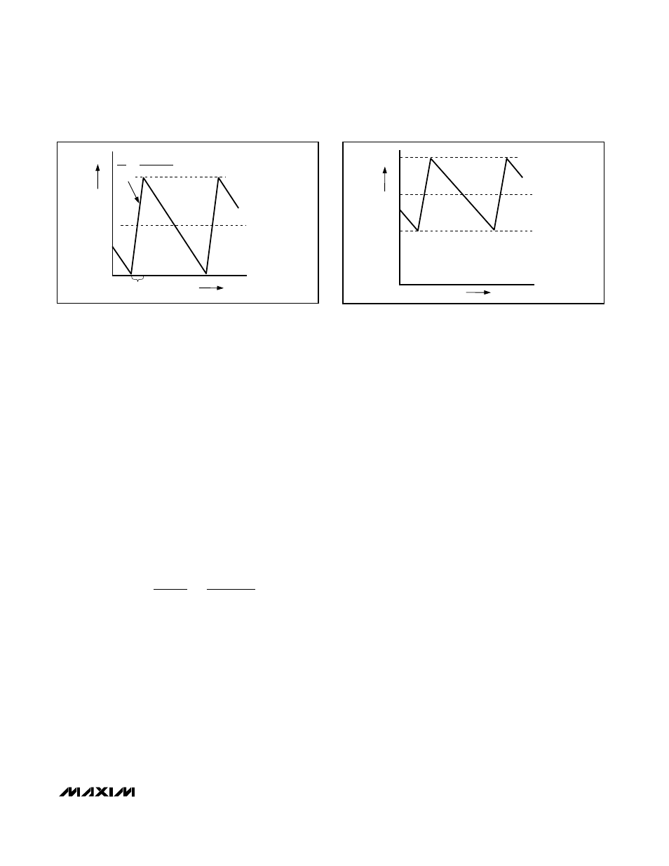
where K is the on-time scale factor (Table 5). The load-
current level at which PFM/PWM crossover occurs,
I
LOAD(SKIP)
, is equal to 1/2 the peak-to-peak ripple cur-
rent, which is a function of the inductor value (Figure 3).
For example, in the standard application circuit with
K = 3.3µs (Table 5), V
OUT
= 2.5V, V
IN
= 15V, and L =
6.8µH, switchover to pulse-skipping operation occurs at
I
LOAD
= 0.51A or about 1/8 full load. The crossover point
occurs at an even lower value if a swinging (soft-satura-
tion) inductor is used.
The switching waveforms may appear noisy and asyn-
chronous when light loading causes pulse-skipping
operation, but this is a normal operating condition that
results in high light-load efficiency. Trade-offs in PFM
noise vs. light-load efficiency are made by varying the
inductor value. Generally, low inductor values produce a
broader efficiency vs. load curve, while higher values
result in higher full-load efficiency (assuming that the coil
resistance remains fixed) and less output voltage ripple.
Penalties for using higher inductor values include larger
physical size and degraded load-transient response
(especially at low input voltage levels).
DC output accuracy specifications refer to the threshold
of the error comparator. When the inductor is in continu-
ous conduction, the output voltage will have a DC regu-
lation level higher than the trip level by 50% of the ripple.
In discontinuous conduction (SKIP = GND, light load),
the output voltage will have a DC regulation level higher
than the error-comparator threshold by approximately
1.5% due to slope compensation.
Forced-PWM Mode (
SKIP
= High)
The low-noise forced-PWM mode (SKIP = high) disables
the zero-crossing comparator, which controls the low-
side switch on-time. This causes the low-side gate-drive
waveform to become the complement of the high-side
gate-drive waveform. This in turn causes the inductor
current to reverse at light loads while DH maintains a
duty factor of V
OUT
/V
IN
. The benefit of forced-PWM
mode is to keep the switching frequency fairly constant,
but it comes at a cost: the no-load battery current can be
10mA to 40mA, depending on the external MOSFETs.
Forced-PWM mode is most useful for reducing audio-
frequency noise, improving load-transient response, pro-
viding sink-current capability for dynamic output voltage
adjustment, and improving the cross-regulation of
multiple-output applications that use a flyback trans-
former or coupled inductor.
I
KV
2L
V
- V
V
LOAD(SKIP)
OUT
IN
OUT
IN
≈
×
MAX1844
High-Speed Step-Down Controller with
Accurate Current Limit for Notebook Computers
______________________________________________________________________________________
13
Figure 3. Pulse-Skipping/Discontinuous Crossover Point
INDUCTOR CURRENT
I
LOAD
= I
PEAK
/2
ON-TIME
0
TIME
I
PEAK
L
V
BATT
-V
OUT
∆
i
∆
t
=
Figure 4. ‘‘Valley’’ Current-Limit Threshold Point
I
LIMIT
I
LOAD
0
TIME
I
PEAK
INDUCTOR CURRENT